 PCB
PCB FPC
FPC Rigid-Flex
 FR-4
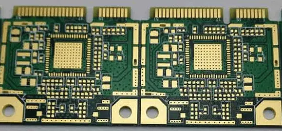
FR-4 HDI PCB
 Rogers High-Frequency Board
 PTFE Teflon High-Frequency Board
 Aluminum
 Copper Core
 PCB Assembly
 LED light PCBA
 Memory PCBA
 Power Supply PCBA
 New Energey PCBA
 Communication PCBA
 Industrial Control PCBA
 Medical Equipment PCBA
 Testing Service
 PCBA Testing Service
 Certification Application
 RoHS Certification Application
 REACH Certification Application
 CE Certification Application
 FCC Certification Application
 CQC Certification Application
 UL Certification Application
 Transformers, Inductors
 High Frequency Transformers
 Low Frequency Transformers
 High Power Transformers
 Conversion Transformers
 Sealed Transformers
 Ring Transformers
 Inductors
 Wires,Cables Customized
 Network Cables
 Power Cords
 Antenna Cables
 Coaxial Cables
 Net Position Indicator
 Solar AIS net position indicator
 Capacitors
 Connectors
 Diodes
 Embedded Processors & Controllers
 Digital Signal Processors (DSP/DSC)
 Microcontrollers (MCU/MPU/SOC)
 Programmable Logic Device(CPLD/FPGA)
 Communication Modules/IoT
 Resistors
 Through Hole Resistors
 Resistor Networks, Arrays
 Potentiometers,Variable Resistors
 Aluminum Case,Porcelain Tube Resistance
 Current Sense Resistors,Shunt Resistors
 Switches
 Transistors
 Power Modules
 Isolated Power Modules
 AC-DC Power Modules
 DC-AC Module(Inverter)
 RF and Wireless
Optimizing Pulse Plating Parameters for Uniform Copper Thickness in High-Aspect-Ratio Through-Holes
In through-holes with aspect ratio>8:1, conventional DC plating shows up to 40% thickness variation (suRFace vs. center). Pulse plating achieves ±10% uniformity via reverse current stripping. This guide details optimization through parametric modeling, bath chemistry, and equipment innovations.
1. Pulse Plating Mechanism & Modeling
1.1 Mass Transport Equation
Ion concentration distribution:
Where:
-
: Ion concentration (mol/cm³)
-
: Diffusion coefficient (6.5×10⁻⁶ cm²/s for Cu²⁺)
-
: Current density (A/cm²)
-
: Electron number (2 for Cu²⁺)
1.2 Key Pulse Parameters
| Parameter | Symbol | Optimal Range | Physical Role |
|---|---|---|---|
| Forward CD | Jₚ | 3-6 ASD | Controls deposition rate |
| Reverse CD | Jᵣ | 1.5-2.5 Jₚ | Strips over-plated surface |
| Forward Time | Tₚ | 10-30 ms | Governs deposit depth |
| Reverse Time | Tᵣ | 0.2-0.5 Tₚ | Determines stripping intensity |
| Off Time | Tₒ | 1-5 ms | Allows ion replenishment |
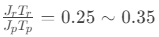
Optimal Ratio: Uniformity peaks at
2. Bath Chemistry & Additives
2.1 Base Solution
| Component | Concentration | Function |
|---|---|---|
| CuSO₄ | 60-80 g/L | Copper ion source |
| H₂SO₄ | 180-220 g/L | Enhances conductivity |
| Cl⁻ | 50-70 ppm | Promotes anode dissolution |
2.2 Additive Synergy
| Additive Type | Example | Dose(mL/L) | Mechanism |
|---|---|---|---|
| Suppressor | PEG-8000 | 1.0-1.5 | Adsorbs at hole opening |
| Leveler | Janus Green B | 0.3-0.5 | Prefers high-current areas |
| Accelerator | SPS | 2.0-3.0 | Boosts bottom deposition |
Synergy: 3:1:4 ratio improves throwing power by 120%
3. Equipment & Process Control
3.1 Pulse Power Supply
| Parameter | Standard DC | Optimized Pulse |
|---|---|---|
| Rise Time | >100 μs | <5 μs |
| Waveform | None | Trapezoidal (adjustable) |
| Multi-Channel Sync | - | ≤1 μs phase error |
3.2 Auxiliary Systems
-
Vibration:
-
30-50Hz, 1-2mm amplitude
-
25% mass transfer improvement
-
-
Pulsed Jet:
-
Flow rate 0.5-1.5m/s, pulse cycle 0.5-2s
-
40% higher ion concentration at hole bottom
-
4. Validation & Process Window
4.1 Thickness Uniformity Inspection
| Method | Location | Accuracy | Metric |
|---|---|---|---|
| XRF Thickness | Top/Mid/Bottom | ±0.1μm | Thickness ratio (Mid/Top) |
| Cross-section | Depth sections | ±0.5μm | Thickness range |
| Impedance Test | Whole board | ±3% | Impedance consistency |
4.2 Process Window (AR=10:1)
| Parameters | Uniformity(σ) | Throwing Power(T.P%) |
|---|---|---|
| Jₚ=4ASD, Jᵣ=8ASD, Tₚ:Tᵣ=10:1 | ±8.2% | 72% |
| Jₚ=5ASD, Jᵣ=10ASD, Tₚ:Tᵣ=5:1 | ±6.5% | 85% |
| Jₚ=6ASD, Jᵣ=15ASD, Tₚ:Tᵣ=3:1 | ±4.7% | 93% |
5. Case Study
5.1 12-Layer HDI Board (0.2mm hole/2.4mm thickness)
| Process | Surface(μm) | Center(μm) | Uniformity |
|---|---|---|---|
| DC Plating | 32.5 | 18.2 | 44.3% |
| Optimized Pulse | 25.7 | 23.6 | 8.2% |
5.2 Reliability Tests
-
Thermal Stress (288℃ solder dip):
-
DC holes: Micro-cracks after 5 cycles
-
Pulse holes: No defects @20 cycles
-
-
Current Loading:
-
35% higher current capacity (30A for 1h)
-
Conclusion
Optimized pulse parameters ( ), additive synergy (PEG-JGB-SPS=3:1:4), and vibration-assisted mass transfer achieve:
-
±5% copper thickness uniformity for AR=10:1
-
90% throwing power
-
4× improvement in thermal reliability
Five Critical Controls:
Reverse Current Law: Jᵣ = 1.8 × J
Golden Time Ratio: T:Tᵣ=5:1 (AR>8:1)
Additive Balance: Real-time suppressor/leveler/accelerator monitoring
Waveform Steepness: Rise/Fall time <5μs
Mass Transfer Enhancement: 30-50Hz vibration + pulsed jet