 PCB
PCB FPC
FPC Rigid-Flex
 FR-4
FR-4 HDI PCB
 Rogers High-Frequency Board
 PTFE Teflon High-Frequency Board
 Aluminum
 Copper Core
 PCB Assembly
 LED light PCBA
 Memory PCBA
 Power Supply PCBA
 New Energey PCBA
 Communication PCBA
 Industrial Control PCBA
 Medical Equipment PCBA
 Testing Service
 PCBA Testing Service
 Certification Application
 RoHS Certification Application
 REACH Certification Application
 CE Certification Application
 FCC Certification Application
 CQC Certification Application
 UL Certification Application
 Transformers, Inductors
 High Frequency Transformers
 Low Frequency Transformers
 High Power Transformers
 Conversion Transformers
 Sealed Transformers
 Ring Transformers
 Inductors
 Wires,Cables Customized
 Network Cables
 Power Cords
 Antenna Cables
 Coaxial Cables
 Net Position Indicator
 Solar AIS net position indicator
 Capacitors
 Connectors
 Diodes
 Embedded Processors & Controllers
 Digital Signal Processors (DSP/DSC)
 Microcontrollers (MCU/MPU/SOC)
 Programmable Logic Device(CPLD/FPGA)
 Communication Modules/IoT
 Resistors
 Through Hole Resistors
 Resistor Networks, Arrays
 Potentiometers,Variable Resistors
 Aluminum Case,Porcelain Tube Resistance
 Current Sense Resistors,Shunt Resistors
 Switches
 Transistors
 Power Modules
 Isolated Power Modules
 AC-DC Power Modules
 DC-AC Module(Inverter)
 RF and Wireless
Optimizing Heat Conduction in High-Power PCB Design
Optimizing Heat Conduction in High-Power Pcb Design Through Copper Thickness, Thermal Vias, and Heat Sink Design. Key Parameters for Thermal Resistance Calculation
In high-power PCB design, thermal management is critical to ensuring circuit reliability and long-term stability. Power devices (e.g., MOSFETs, IGBTs, power ICs) generate significant heat during operation. Poor heat dissipation can lead to temperature rise, peRFormance degradation, or even device failure. Below are methods to optimize heat conduction through copper thickness, thermal vias, and heat sink design, along with key parameters for thermal resistance calculations.
I. Key Design Methods to Optimize Heat Conduction
1. Copper Thickness Optimization
Copper, with its high thermal conductivity (~385 W/m·K), is the primary heat-conducting material in PCBs. Increasing copper thickness enhances heat dissipation.
Optimization Strategies:
-
Thick Copper for High-Current Paths: Use 2 oz (70 μm) or thicker copper for high-power traces or power planes to reduce resistive losses (Joule heating) and improve lateral heat spreading.
-
Copper Layer Layout: Place large copper pours under heat-generating components and stack multiple copper layers (e.g., power/ground planes) to create 3D heat dissipation paths.
-
Cost-Benefit Balance: Thicker copper increases etching complexity and cost; optimize based on power density and thermal requirements.
2. Thermal Via Design
Thermal vias transfer heat vertically from components to other PCB layers or heat sinks.
Optimization Strategies:
-
Dense Arrays: Deploy high-density via arrays (e.g., 0.3 mm diameter, 0.6 mm pitch) under or around heat sources to minimize thermal resistance.
-
Filling and Plating: Fill vias with conductive epoxy or resin and increase via wall copper thickness (≥25 μm) to reduce air gaps and thermal resistance.
-
Thermal Connections: Link vias to internal copper planes or backside heat sinks to establish "thermal pathways."
3. Heat Sink Integration
Heat sinks enhance heat dissipation by increasing surface area and enabling forced convection.
Optimization Strategies:
-
Direct Mounting: Attach heat sinks to components using thermal adhesive, screws, or clips. Ensure flat contact surfaces (apply thermal grease if needed).
-
Embedded Heat Sinks: Use metal-core substrates (e.g., aluminum or copper) or embedded metal blocks (MCPCB) for extreme power applications.
-
Finned Designs: Employ finned heat sinks to maximize surface area, paired with fans for forced airflow.
II. Key Parameters for Thermal Resistance Calculation
Thermal resistance (, in °C/W) quantifies the impediment to heat flow. Total thermal resistance is the sum of resistances across the heat transfer path:

Critical Parameters:
1. Junction-to-Case Thermal Resistance ()
-
Definition: Resistance from the device junction to its case, determined by packaging materials and structure.
-
Typical Values: 1–5°C/W for power MOSFETs (refer to datasheets).
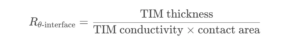
2. Interface Thermal Resistance ()
-
Factors:
-
Surface roughness: Air gaps from rough surfaces increase resistance.
-
Thermal interface material (TIM): Thermal grease (~0.1°C·cm²/W) outperforms air (~5°C·cm²/W).
-
-
Formula:
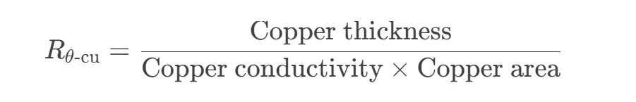
3. PCB Internal Thermal Resistance (��-pcb)
-
Copper Layer Resistance:
-
Via Resistance:
Example: 10 copper-filled vias (0.3 mm diameter, 1.6 mm length) yield ~0.08°C/W total resistance.

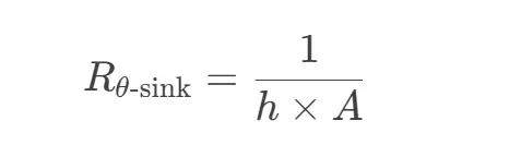
4. Heat Sink-to-Ambient Resistance (��-sink)
-
Natural Convection: Depends on surface area and emissivity; typical range: 5–20°C/W.
-
Forced Convection: With fans, resistance drops to 1–5°C/W.
-
Formula:
ℎ: Convection coefficient (5–25 W/m²·K for natural, up to 100 W/m²·K for forced).
: Effective heat sink surface area.
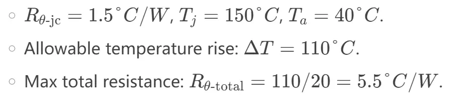
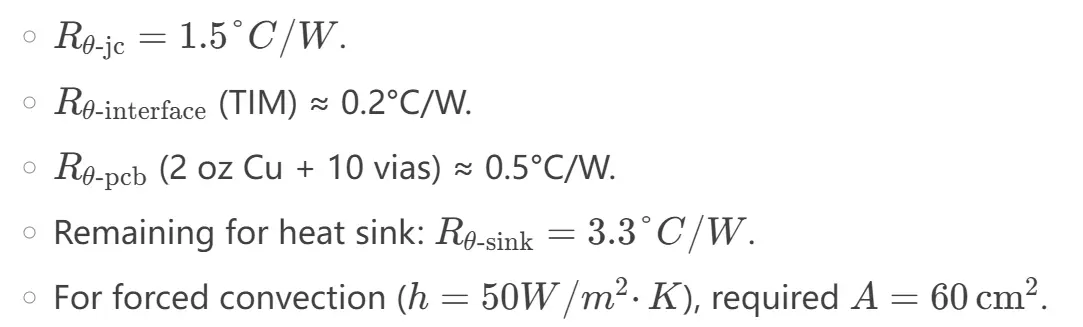
III. Design Example and Tradeoffs
Case Study: 20W MOSFET Thermal Design
-
Device Parameters:
-
Thermal Budget Allocation:
IV. Key Takeaways
-
Copper Optimization: Thicker copper layers reduce lateral resistance.
-
Thermal Vias: High-density, filled vias minimize vertical resistance.
-
Heat Sinks: Balance surface area and convection methods for efficiency.
-
Thermal Modeling: Use hierarchical resistance models and simulation tools (e.g., ANSYS Icepak) for validation.
In practice, combine thermal simulations with infrared thermography to ensure alignment between theoretical predictions and real-world performance.