 PCB
PCB FPC
FPC Rigid-Flex
 FR-4
FR-4 HDI PCB
 Rogers High-Frequency Board
 PTFE Teflon High-Frequency Board
 Aluminum
 Copper Core
 PCB Assembly
 LED light PCBA
 Memory PCBA
 Power Supply PCBA
 New Energey PCBA
 Communication PCBA
 Industrial Control PCBA
 Medical Equipment PCBA
 Testing Service
 PCBA Testing Service
 Certification Application
 RoHS Certification Application
 REACH Certification Application
 CE Certification Application
 FCC Certification Application
 CQC Certification Application
 UL Certification Application
 Transformers, Inductors
 High Frequency Transformers
 Low Frequency Transformers
 High Power Transformers
 Conversion Transformers
 Sealed Transformers
 Ring Transformers
 Inductors
 Wires,Cables Customized
 Network Cables
 Power Cords
 Antenna Cables
 Coaxial Cables
 Net Position Indicator
 Solar AIS net position indicator
 Capacitors
 Connectors
 Diodes
 Embedded Processors & Controllers
 Digital Signal Processors (DSP/DSC)
 Microcontrollers (MCU/MPU/SOC)
 Programmable Logic Device(CPLD/FPGA)
 Communication Modules/IoT
 Resistors
 Through Hole Resistors
 Resistor Networks, Arrays
 Potentiometers,Variable Resistors
 Aluminum Case,Porcelain Tube Resistance
 Current Sense Resistors,Shunt Resistors
 Switches
 Transistors
 Power Modules
 Isolated Power Modules
 AC-DC Power Modules
 DC-AC Module(Inverter)
 RF and Wireless
What technologies are mainly used in PCB multilayer boards?
What technologies are mainly used in PCB multilayer boards?
In the vast field of hardware engineering, the design and manufacture of multilayer Pcb Boards undoubtedly constitute a complex and intricate branch. For engineers who are new to this field, the internal structural complexity of multilayer PCB boards, especially those with up to ten or even more layers, is often breathtaking.
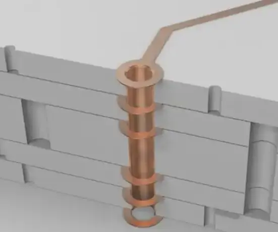
The manufacturing of multilayer PCB boards does not differ significantly from single-layer or double-layer boards in terms of etched circuitry; however, the true challenge lies in the fabrication process of vias. Via technology, as the core of High-Density Interconnect (HDI) boards, is achieved by drilling holes in the board and plating them with copper. This seemingly simple process has a crucial impact on the peRFormance and reliability of multilayer PCB boards.
Among the classifications of multilayer PCB boards, the common types include through-hole boards, first-order boards, second-order boards, and second-order stacked via boards. Through-hole boards are the foundation of all multilayer PCB boards, characterized by holes that penetrate all layers, whether for external or internal circuitry. This design allows current to flow freely between different layers, thereby enhancing the overall performance of the circuit board. However, as the number of layers increases, the manufacturing difficulty and cost of through-hole boards also increase accordingly.
To address this challenge, high-density boards (HDI boards) emerged. HDI boards use laser technology to drill holes in the surface layer with diameters as small as 0.1mm. These laser holes only penetrate the board material without affecting the internal copper layers, allowing for drilling on the outer surface without interfering with internal circuitry. The advent of this technology has greatly increased the wiring density and signal transmission speed of multilayer PCB boards.
Building upon HDI boards, second-order HDI boards and stacked via boards further advanced the development of multilayer PCB board technology. Second-order HDI boards feature two layers of laser holes, typically used in PCB designs with eight or more layers. This design not only increases wiring density but also enhances the connection reliability and durability of the circuit board through the "staggered via" technology, which allows for copper plating within the holes. Stacked via boards are even more complex, with two layers of laser holes overlapping in position, making the circuit layout more compact. However, this design also brings higher manufacturing costs and processing difficulties.
Any-layer interconnect boards represent the pinnacle of multilayer PCB board technology. Each layer of this type of PCB board can have laser holes, achieving extremely high design freedom. Due to their extremely high manufacturing costs, they are usually only adopted in high-end products. Nevertheless, it is this technological breakthrough that makes it possible to enhance the performance and reduce the size of electronic devices.
As the number of PCB layers increases and via technology becomes more complex, the design and manufacturing costs of PCBs also rise accordingly. Therefore, choosing the right manufacturing factory becomes particularly important. Minintel is a precision factory specializing in high-level multilayer PCB processing, with dedicated production lines and specialized processing and testing equipment for HDI processing. These advanced production equipment and technological means ensure that PCBs can be manufactured with high precision and quality.