 PCB
PCB FPC
FPC Rigid-Flex
 FR-4
FR-4 HDI PCB
 Rogers High-Frequency Board
 PTFE Teflon High-Frequency Board
 Aluminum
 Copper Core
 PCB Assembly
 LED light PCBA
 Memory PCBA
 Power Supply PCBA
 New Energey PCBA
 Communication PCBA
 Industrial Control PCBA
 Medical Equipment PCBA
 Testing Service
 PCBA Testing Service
 Certification Application
 RoHS Certification Application
 REACH Certification Application
 CE Certification Application
 FCC Certification Application
 CQC Certification Application
 UL Certification Application
 Transformers, Inductors
 High Frequency Transformers
 Low Frequency Transformers
 High Power Transformers
 Conversion Transformers
 Sealed Transformers
 Ring Transformers
 Inductors
 Wires,Cables Customized
 Network Cables
 Power Cords
 Antenna Cables
 Coaxial Cables
 Net Position Indicator
 Solar AIS net position indicator
 Capacitors
 Connectors
 Diodes
 Embedded Processors & Controllers
 Digital Signal Processors (DSP/DSC)
 Microcontrollers (MCU/MPU/SOC)
 Programmable Logic Device(CPLD/FPGA)
 Communication Modules/IoT
 Resistors
 Through Hole Resistors
 Resistor Networks, Arrays
 Potentiometers,Variable Resistors
 Aluminum Case,Porcelain Tube Resistance
 Current Sense Resistors,Shunt Resistors
 Switches
 Transistors
 Power Modules
 Isolated Power Modules
 AC-DC Power Modules
 DC-AC Module(Inverter)
 RF and Wireless
Achieving Reliable Flex Cycle Life Testing for Wearable Electronics PCBs
2025-12-14
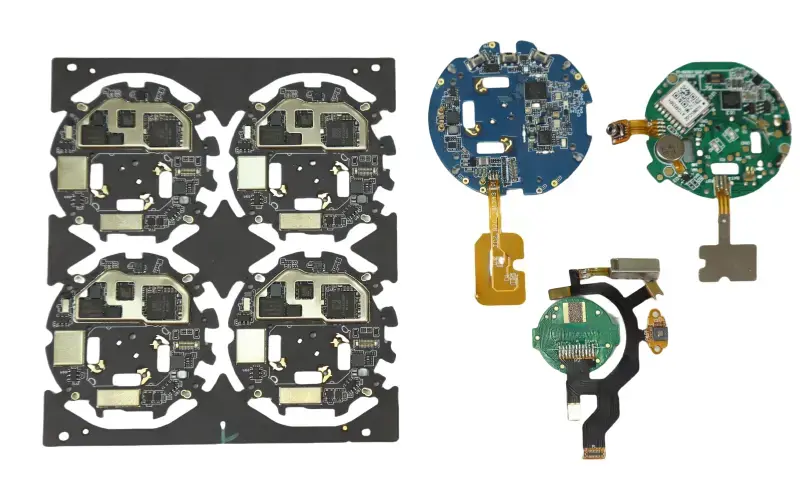
Wearable electronics—including smartwatches, fitness trackers, medical monitoring patches, and augmented reality headsets—rely on flexible and rigid-flex printed circuit boards (PCBs) to deliver compact, lightweight, and body-conformable designs. Unlike traditional Rigid Pcbs, wearable PCBs are subjected to repeated mechanical bending during daily use, whether from wrist movement, joint flexion, or fabric stretching. Over time, this cyclic bending can cause copper trace fatigue, solder joint cracking, and substrate delamination, leading to premature device failure. Flex cycle life testing is a critical reliability validation process that SIMulates real-world bending conditions to quantify a wearable PCB’s durability and identify potential failure points. This article provides a comprehensive, step-by-step guide to designing and executing a rigorous flex cycle life testing program for wearable electronics PCBs, aligned with international standards such as IPC-6013 (Specification for Flexible Printed Boards) and IEC 60068-2-27 (Environmental Testing for Electronic Products). It covers test specimen preparation, equipment selection, parameter setting, failure detection, and data analysis, with a focus on the unique requirements of wearable applications.
1. Fundamentals of Wearable PCB Flex Fatigue and Failure Mechanisms
To design an effective flex cycle life test, it is first essential to understand the mechanical stresses that wearable PCBs endure and the failure modes that result from cyclic bending.
1.1 Mechanical Stress in Wearable PCBs
Wearable PCBs are typically constructed with flexible substrates (e.g., polyimide, PI) and thin copper traces (12–35μm), bonded to rigid sections (e.g., FR-4) for component mounting—a structure known as rigid-flex PCB. During bending, two primary types of stress act on the PCB:
- Tensile Stress: Applied to the outer surface of the bent PCB, stretching copper traces and substrate materials. Excessive tensile stress causes trace elongation and eventual fracture.
- Compressive Stress: Applied to the inner surface of the bent PCB, compressing traces and potentially causing buckling or delamination between the copper and substrate layers.
The magnitude of these stresses depends on three key factors:
- Bending Radius: The radius of the curve formed during bending. Smaller bending radii (e.g., 5mm for a smartwatch band) create higher stress levels than larger radii (e.g., 20mm for a chest strap).
- Bending Angle: The degree of deflection from the PCB’s flat state, typically ranging from 0° (flat) to 180° (folded) for wearable devices.
- Cycle Count: The number of repeated bending cycles. Wearable PCBs are expected to withstand 10,000–1,000,000 cycles, depending on the application (e.g., 100,000 cycles for a smartwatch with a 2-year lifespan).
1.2 Common Flex Fatigue Failure Modes
Cyclic bending induces progressive damage in wearable PCBs, leading to distinct failure modes that must be targeted during testing:
- Copper Trace Fracture: The most common failure mode, caused by fatigue cracks propagating through copper traces. This typically occurs at trace corners, vias, or areas where trace width changes abruptly.
- Solder Joint Cracking: Rigid components (e.g., ICs, connectors) mounted on flexible sections experience high stress during bending, leading to cracks in solder joints. This is a critical failure mode for wearable devices with surface-mount components (SMDs).
- Substrate Delamination: The bond between the copper trace and flexible substrate weakens over time, causing delamination. This can lead to intermittent electrical connections or complete trace detachment.
- Via Failure: Plated through-holes (PTHs) in rigid-flex PCBs are prone to cracking at the interface between rigid and flexible sections, as this area experiences maximum stress concentration.
A study by the IEEE Wearable Electronics Technical Committee found that 65% of wearable device field failures are attributed to flex fatigue, with copper trace fracture accounting for 40% of these failures. This underscores the importance of rigorous flex cycle life testing in wearable PCB design validation.
2. Test Specimen Preparation: Critical Steps for Accurate Results
The quality of test specimens directly impacts the validity of flex cycle life test results. Wearable PCB test specimens must replicate the design, materials, and assembly processes of the final product to ensure realistic stress distribution.
2.1 Specimen Design Requirements
- Dimensional Consistency: Specimens must match the exact dimensions of the wearable PCB’s flexible sections, including trace width, copper thickness, substrate thickness, and via placement. For rigid-flex PCBs, the rigid-flex transition zone—where stress is concentrated—must be included in the specimen.
- Representative Trace Layout: Include critical trace paths (e.g., power, signal, ground) that are most susceptible to failure. Avoid adding test-specific features (e.g., extra vias) that alter the PCB’s mechanical behavior.
- Component Assembly: Mount the same SMDs and connectors used in the final product, using the same solder paste, reflow profile, and adhesive materials. Unassembled PCBs can be tested to isolate substrate and trace fatigue, but assembled specimens are required to validate solder joint reliability.
- Sample Size: Test a minimum of 5–10 specimens per PCB design to account for manufacturing variability. This allows for statistical analysis of failure rates and cycle life distribution.
2.2 Specimen Preparation Procedures
- PCB Fabrication: Manufacture test specimens using the same production process as the final product, including substrate lamination, copper etching, via plating, and solder mask application. Ensure that key parameters (e.g., copper thickness, adhesive layer thickness) are within specification.
- Component Assembly: Solder components to the specimens using the standard reflow profile for wearable devices (typically low-temperature solder pastes to avoid damaging flexible substrates). Use underfill or adhesive for large components (e.g., microcontrollers) to simulate real-world assembly.
- Pre-Test Inspection: Conduct a thorough pre-test inspection to eliminate defective specimens:
- Visual Inspection: Check for trace defects, delamination, or solder joint anomalies using a digital microscope (10–50x magnification).
- Electrical Continuity Test: Verify that all traces and components have continuous electrical connections using a multimeter or in-circuit tester (ICT).
- Dimensional Measurement: Measure the bending radius and trace dimensions of each specimen to ensure consistency, using a coordinate measuring machine (CMM) for high precision.
3. Equipment Selection for Wearable PCB Flex Cycle Life Testing
The choice of testing equipment depends on the type of bending that the wearable PCB experiences in real use. Three primary test methods are used for wearable electronics, each with specialized equipment.
3.1 Bending Test Methods and Corresponding Equipment
| Test Method | Equipment Type | Wearable Application Scenario | Key Advantages |
|---|---|---|---|
| Dynamic Bending Test | Motorized flex test machine (e.g., Instron 5940, MTS Insight) | Smartwatch bands, wrist straps (repeated bending around a fixed radius) | Simulates continuous cyclic bending; precise control of bending radius and cycle rate |
| Torsion Bending Test | Torsion flex test fixture | Fitness tracker bands, fabric-integrated PCBs (twisting and bending combined) | Replicates multi-axial stress from body movement; ideal for stretchable wearables |
| Creep Bending Test | Constant-load flex fixture with environmental chamber | Medical patches, skin-worn sensors (prolonged static bending with temperature cycling) | Evaluates long-term creep fatigue; incorporates temperature and humidity effects |
3.2 Key Equipment Features for Wearable PCBs
- Bending Radius Adjustability: Wearable PCBs require small bending radii (2–15mm), so the test equipment must support precise radius adjustments down to 2mm.
- Cycle Rate Control: The test cycle rate should be 10–60 cycles per minute (CPM). Faster rates (e.g., 60 CPM) reduce test duration but may induce additional thermal stress; slower rates (e.g., 10 CPM) better simulate real-world use.
- Environmental Control: Many wearable devices operate in harsh environments (e.g., high humidity for fitness trackers, body temperature for medical patches). The test equipment should integrate an environmental chamber to control temperature (25–40°C) and relative humidity (30–90%) during testing.
- In-Situ Monitoring: Advanced test machines include electrical continuity monitoring to detect trace or solder joint failures in real time, eliminating the need for manual inspection during testing.
4. Defining Test Parameters: Aligning with Wearable Application Requirements
Test parameters must be tailored to the specific use case of the wearable device, as different applications experience distinct bending conditions. The following parameters are defined based on IPC-6013 and IEC 60068-2-27 standards, with adjustments for wearable-specific stress levels.
4.1 Core Test Parameters and Recommended Ranges
| Parameter | Definition | Wearable-Specific Range | Standard Compliance |
|---|---|---|---|
| Bending Radius (R) | The radius of the mandrel around which the PCB is bent | 2–15mm (depends on device: 2–5mm for smartwatches; 10–15mm for chest straps) | IPC-6013 §3.8.2 |
| Bending Angle (θ) | The angle of deflection from flat | 90°–180° (full flexion for wrist wearables; 90° for chest wearables) | IEC 60068-2-27 §5.2 |
| Cycle Rate (CR) | Number of bending cycles per minute | 10–30 CPM (slower rate to avoid thermal buildup) | IPC-6013 §4.5.1 |
| Cycle Count (N) | Total number of cycles to test | 10,000–1,000,000 cycles (100,000 cycles for consumer wearables; 1,000,000 cycles for medical devices) | IEC 60068-2-27 §5.3 |
| Temperature (T) | Ambient temperature during testing | 25°C (room temperature) or 37°C (body temperature for medical wearables) | IPC-6013 §4.4.2 |
| Relative Humidity (RH) | Humidity level during testing | 30–60% RH (consumer wearables); 60–90% RH (outdoor fitness trackers) | IEC 60068-2-78 |
4.2 Parameter Setting Guidelines for Common Wearable Applications
4.2.1 Smartwatch PCB Test Parameters
- Bending Radius: 3–5mm (matches the curvature of a wrist)
- Bending Angle: 180° (full flexion of the watch band)
- Cycle Rate: 20 CPM
- Cycle Count: 100,000 cycles (equivalent to 2 years of daily use)
- Environment: 25°C, 50% RH
4.2.2 Medical Patch PCB Test Parameters
- Bending Radius: 5–8mm (matches skin curvature on the arm or chest)
- Bending Angle: 90° (mimics body joint movement)
- Cycle Rate: 10 CPM
- Cycle Count: 500,000 cycles (equivalent to 5 years of medical device use)
- Environment: 37°C, 60% RH (simulates body temperature and humidity)
4.2.3 Fitness Tracker PCB Test Parameters
- Bending Radius: 8–12mm (matches the curvature of a forearm)
- Bending Angle: 120° (flexion during exercise)
- Cycle Rate: 30 CPM
- Cycle Count: 200,000 cycles (equivalent to 1 year of intense use)
- Environment: 30°C, 80% RH (simulates outdoor exercise conditions)
4.3 Critical Parameter Adjustments for Rigid-Flex PCBs
Rigid-flex PCBs require additional parameter considerations due to the stress concentration at the rigid-flex transition zone:
- Bending Axis Alignment: Align the bending axis with the rigid-flex transition zone to maximize stress on this critical area.
- Load Application: Apply a small tensile load (0.1–0.5 N) to the specimen during testing to simulate the tension from wearable device straps.
- Cycle Pause Interval: For long-duration tests (e.g., 1,000,000 cycles), include a 5-minute pause every 10,000 cycles to allow the PCB to cool, preventing thermal fatigue from cycle rate-induced heating.
5. Test Execution and In-Process Monitoring
Executing the flex cycle life test requires strict adherence to the defined parameters and continuous monitoring to detect failures early and collect accurate data.
5.1 Step-by-Step Test Execution Process
- Specimen Mounting: Secure the test specimen to the flex test machine’s fixtures, ensuring that the bending radius and axis are aligned correctly. For rigid-flex PCBs, clamp the rigid sections to the fixtures to isolate bending stress in the flexible sections.
- Parameter Calibration: Set the bending angle, cycle rate, temperature, and humidity on the test equipment. Run a 100-cycle pre-test to verify that the parameters are applied correctly and that the specimen is not slipping in the fixtures.
- In-Situ Monitoring Setup: Connect the specimen to an electrical continuity monitor to track resistance changes in critical traces and solder joints. Set a resistance threshold (e.g., 10Ω above the initial resistance) to trigger a failure alert.
- Full Test Execution: Start the test and run it for the specified cycle count, or until all specimens fail. Record cycle count, temperature, humidity, and resistance data at 10,000-cycle intervals.
- Interim Inspection: For tests exceeding 100,000 cycles, pause the test every 50,000 cycles to conduct a visual inspection of the specimens. Check for trace cracks, delamination, or solder joint damage using a digital microscope.
5.2 Failure Detection and Classification
Failures are classified based on the failure mode and the cycle count at which they occur:
- Early Failure (0–10,000 cycles): Indicates a design or manufacturing defect (e.g., poor trace adhesion, solder joint voids). These specimens are excluded from statistical analysis.
- Normal Failure (10,000–1,000,000 cycles): Indicates fatigue failure due to cyclic bending. These failures are used to calculate the PCB’s mean time to failure (MTTF).
- No Failure (>1,000,000 cycles): Indicates that the PCB exceeds the required durability. These specimens can be subjected to accelerated testing (e.g., smaller bending radius) to determine the maximum cycle life.
For each failed specimen, document the following information:
- Cycle count at failure
- Failure mode (trace fracture, solder joint cracking, etc.)
- Failure location (rigid-flex transition zone, trace corner, etc.)
- Resistance change at failure
6. Data Analysis and Test Report Generation
The final step in flex cycle life testing is analyzing the collected data to evaluate the PCB’s durability and identify opportunities for design improvement.
6.1 Statistical Data Analysis
- Mean Time to Failure (MTTF): Calculate the average cycle count at which specimens fail. For wearable PCBs, the MTTF should be at least 2x the required cycle count to ensure a safety margin.
- Failure Rate Distribution: Plot the failure rate against cycle count using a Weibull distribution graph. This graph identifies the failure mode distribution and the cycle count at which 10%, 50%, and 90% of specimens fail (known as B10, B50, B90 life).
- Stress vs. Cycle Count Relationship: Conduct a series of tests with different bending radii to establish a stress-cycle (S-N) curve. This curve quantifies how reducing the bending radius (increasing stress) decreases the PCB’s cycle life.
6.2 Test Report Requirements
A comprehensive test report should include the following sections, aligned with IPC and IEC standards:
- Test Overview: Purpose of the test, PCB design details, and specimen information.
- Test Equipment and Parameters: Equipment model, bending radius, cycle rate, temperature, humidity, and cycle count.
- Test Results: MTTF, Weibull distribution data, failure mode classification, and failure location maps.
- Failure Analysis: Microscope images of failed specimens, root cause analysis (e.g., trace width too narrow, solder joint insufficient), and design improvement recommendations.
- Conclusion: Pass/fail determination based on the required cycle life, and recommendations for design optimization or additional testing.
6.3 Design Optimization Based on Test Results
Test results provide actionable insights to improve wearable PCB durability:
- Trace Design Optimization: Widen narrow traces that failed, or add rounded corners to reduce stress concentration.
- Rigid-Flex Transition Zone Improvement: Increase the length of the transition zone or add reinforcing adhesive to reduce stress.
- Component Mounting Optimization: Use underfill or adhesive for SMDs on flexible sections to improve solder joint reliability.
- Substrate Material Selection: Switch to a more durable substrate (e.g., thicker polyimide) if delamination is a common failure mode.
7. Conclusion
Flex cycle life testing is an indispensable process for validating the reliability of wearable electronics PCBs, as it simulates the repeated bending stress that these boards experience in real-world use. By following the systematic approach outlined in this article—from specimen preparation and equipment selection to parameter setting, test execution, and data analysis—engineers can accurately quantify a wearable PCB’s durability, identify critical failure modes, and optimize designs to meet the stringent reliability requirements of wearable applications.
As wearable electronics continue to evolve toward more flexible, stretchable, and body-conformable designs, flex cycle life testing will become even more critical. Emerging technologies, such as stretchable conductive inks and self-healing substrates, will require new test methods to evaluate their unique fatigue properties. However, the core principles of stress simulation, failure detection, and data-driven optimization will remain the foundation of reliable wearable PCB design validation. By prioritizing flex cycle life testing in the design process, wearable device manufacturers can deliver products that are not only innovative and user-friendly but also durable enough to withstand years of daily use.