 PCB
PCB FPC
FPC Rigid-Flex
 FR-4
FR-4 HDI PCB
 Rogers High-Frequency Board
 PTFE Teflon High-Frequency Board
 Aluminum
 Copper Core
 PCB Assembly
 LED light PCBA
 Memory PCBA
 Power Supply PCBA
 New Energey PCBA
 Communication PCBA
 Industrial Control PCBA
 Medical Equipment PCBA
 Testing Service
 PCBA Testing Service
 Certification Application
 RoHS Certification Application
 REACH Certification Application
 CE Certification Application
 FCC Certification Application
 CQC Certification Application
 UL Certification Application
 Transformers, Inductors
 High Frequency Transformers
 Low Frequency Transformers
 High Power Transformers
 Conversion Transformers
 Sealed Transformers
 Ring Transformers
 Inductors
 Wires,Cables Customized
 Network Cables
 Power Cords
 Antenna Cables
 Coaxial Cables
 Net Position Indicator
 Solar AIS net position indicator
 Capacitors
 Connectors
 Diodes
 Embedded Processors & Controllers
 Digital Signal Processors (DSP/DSC)
 Microcontrollers (MCU/MPU/SOC)
 Programmable Logic Device(CPLD/FPGA)
 Communication Modules/IoT
 Resistors
 Through Hole Resistors
 Resistor Networks, Arrays
 Potentiometers,Variable Resistors
 Aluminum Case,Porcelain Tube Resistance
 Current Sense Resistors,Shunt Resistors
 Switches
 Transistors
 Power Modules
 Isolated Power Modules
 AC-DC Power Modules
 DC-AC Module(Inverter)
 RF and Wireless
Part V: Wave Soldering - Formation and Application of Wave Dynamics Theory
Part V: Wave Soldering - Formation and ApplICation of Wave Dynamics Theory
Section 9: Determination of the Optimal Entry Angle (Inclination Angle) Range
Entering at a certain angle can also reduce the size of the boundary layer, with the core principle being the alteration of fluid velocity. Figure 2.12 illustrates the changes in fluid velocity as it enters the working section. The length of the arrowed line segments in the diagram indicates the velocity magnitude at each point, while the direction of the arrows represents the flow direction. As the fluid slides down along the nozzle, its velocity gradually increases, and the angle between its direction and the horizontal also becomes larger. When the PCB enters, the inclination angle increases from α1 to α2, shifting the working section where the PCB cuts into the wave peak from the low-speed A-A segment to the high-speed A′-A′ segment. Obviously, the effect of changing the inclination angle is identical to that of altering the fluid velocity, and thus no further analysis is needed here.
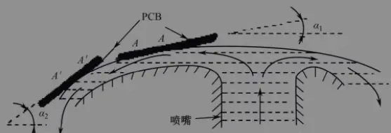
Impact of Inclination Angle on Wave Soldering Effectiveness
Relevant research reports indicate that the friction characteristic of the solder during wave soldering is approximately 3°. Therefore, setting the conveyor inclination angle at 4° to 9° allows the solder to better peel off the PCB suRFace and return to the wave peak. Based on comprehensive experimental analysis, it is generally believed that an inclination angle of 6° to 7° is optimal.
Section 10: Relationship Between Wave Height and Wave Pressure, and Their Impact on Wave Soldering Effectiveness
The wave height depends on the pressure that the pump can generate. In other words, the higher the wave, the greater the pressure required from the pump. Pressure is generally proportional to the square of the fluid velocity within the pump, so as pressure increases, velocity increases more rapidly. An increase in the Reynolds number may cause the fluid to enter a turbulent state, leading to wave instability and an increase in pressure on the wave peak. When the wave height is low, the fluid velocity within the pump is slow and laminar, resulting in a stable wave peak with little fluctuation and consequently lower pressure on the wave peak.
The relationship between wave height, solder flow velocity, and pressure is illustrated in the diagram below.
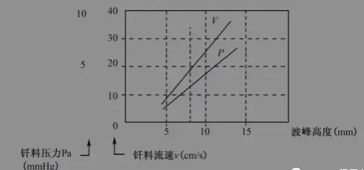
For example, when the wave height is 10mm, the jet pressure of the wave peak on the PCB is approximately 4.78 mmHg, with a flow velocity of 26.6 cm/s. When the wave height is 8mm, the jet pressure drops to 2.45 mmHg, and the flow velocity is 19.0 cm/s. Some believe that the higher the wave jet pressure, the better, which is incorrect, as excessive pressure can cause the solder to jet onto non-soldered surfaces of the PCB. Meanwhile, according to welding principles, welding primarily relies on the wetting action of the solder on the base metal and capillary action to form a joint, and joints formed through such a metallurgical process are the most reliable. While appropriate jet pressure can accelerate wetting, attempting to fill welds by increasing jet pressure may obscure incompletely wetted welds, making them difficult to detect and leaving potential issues. From the perspective of solder wave dynamics, the optimal working height of the solder wave is 6 to 7 mm.
Section 11: Basis for Selecting the Optimal Volume of the Solder Bath
There are diverse opinions on the selection of the solder bath volume. Some argue that the larger the volume, the better, while others claim the opposite. These views are one-sided. In fact, for a certain wave width and breadth, there corresponds an optimal volume, determined by the dynamics of the solder wave. When designing the volume of the solder bath, the first step is to determine the solder circulation coefficient of the solder bath based on fluid dynamics analysis. The solder circulation coefficient can be defined as:
Solder Circulation Coefficient = Mass of solder above the liquid surface / Total mass of solder in the bath
The value of this coefficient varies with different machine designs, and it is confidential among manufacturers in design calculations. The value of the solder circulation coefficient directly affects the overall performance of the solder wave generator. For example, when the shape and structure of the solder wave have been set, i.e., when the mass of solder above the liquid surface during operation is known, the size of the solder circulation coefficient determines the volume of the solder bath.
The smaller the coefficient, the larger the volume. The advantages of a large volume include high thermal capacity, small temperature fluctuations during operation, small liquid surface fluctuations, and easy wave stability. However, this can lead to high solder consumption, high power consumption, and difficulty in achieving dynamic balance in impurity metal concentration during operation, resulting in the accumulation of metallic impurities and easily creating dead zones for deposition and segregation phases, leading to uneven distribution of solder composition within the bath. When metallic impurities accumulate to the allowable limit, the entire bath of solder must be replaced, causing greater losses.
Conversely, when the coefficient is too large, the volume of the solder bath is small, and the situation is the opposite of the above. Therefore, during design calculations, a compromise is generally made between these two extreme cases, with values selected based on overall design and economic requirements to optimize the final combined effect and performance. Thus, it cannot be unilaterally stated that a large volume is better or a small volume is better.
Part IV: The formation and application of wave soldering wave dynamics theory
Part III:Wave Soldering - Formation and Application of Wave Dynamics Theory