 PCB
PCB FPC
FPC Rigid-Flex
 FR-4
FR-4 HDI PCB
 Rogers High-Frequency Board
 PTFE Teflon High-Frequency Board
 Aluminum
 Copper Core
 PCB Assembly
 LED light PCBA
 Memory PCBA
 Power Supply PCBA
 New Energey PCBA
 Communication PCBA
 Industrial Control PCBA
 Medical Equipment PCBA
 Testing Service
 PCBA Testing Service
 Certification Application
 RoHS Certification Application
 REACH Certification Application
 CE Certification Application
 FCC Certification Application
 CQC Certification Application
 UL Certification Application
 Transformers, Inductors
 High Frequency Transformers
 Low Frequency Transformers
 High Power Transformers
 Conversion Transformers
 Sealed Transformers
 Ring Transformers
 Inductors
 Wires,Cables Customized
 Network Cables
 Power Cords
 Antenna Cables
 Coaxial Cables
 Net Position Indicator
 Solar AIS net position indicator
 Capacitors
 Connectors
 Diodes
 Embedded Processors & Controllers
 Digital Signal Processors (DSP/DSC)
 Microcontrollers (MCU/MPU/SOC)
 Programmable Logic Device(CPLD/FPGA)
 Communication Modules/IoT
 Resistors
 Through Hole Resistors
 Resistor Networks, Arrays
 Potentiometers,Variable Resistors
 Aluminum Case,Porcelain Tube Resistance
 Current Sense Resistors,Shunt Resistors
 Switches
 Transistors
 Power Modules
 Isolated Power Modules
 AC-DC Power Modules
 DC-AC Module(Inverter)
 RF and Wireless
Part III:Wave Soldering - Formation and Application of Wave Dynamics Theory
Part III: Wave Soldering - Formation and ApplICation of Wave Dynamics Theory
Section Five: SuRFace Tension of Molten Solder After Dual-Wave Peak
To understand how dual-wave nozzles minimize solder joint protrusion, it is crucial to first comprehend the phenomenon of surface tension and its relationship with wetting. When surface tension fails to wet a surface, it causes the molten solder to form into small spheres. Surface tension controls the wetting condition of a liquid on a surface, thereby controlling how the solder wets the flux-coated base metal surface. In the diagram below, you can see the PCB passing through a dual-wave peak. The solder has wetted the copper foil surface of the PCB and is being dragged out from the wave peak to form a thin layer. The size of this thin layer is controlled by several factors, such as the surface tension of the solder, the velocity characteristics at the point where the wave peak contacts the thin layer of solder, and the mass of the molten solder thin layer at that point.
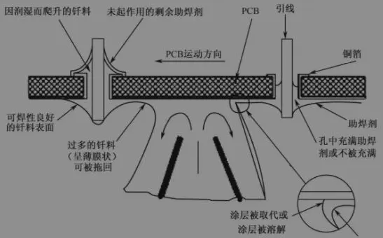
The larger the thin layer's area, the more difficult it is for the surface tension of the molten solder wave peak to drag excess solder back into the wave peak. When the size of the thin layer reaches a certain limit, surface tension will separate them. If excess solder is not dragged back into the wave peak at this point, solder joint protrusion will form. From this very simplified model, it can be seen that our goal is to minimize the area of the thin layer of solder. The methods adopted are as follows:
● Altering the surface tension effect of the solder;
● Changing the velocity characteristics of the wave peak at the point where the thin layer of solder is produced.
There are many ways to achieve the above goals. The surface tension of the solder is affected by its temperature. Higher temperatures reduce surface tension, but increased temperatures intensify the oxidation of the molten solder surface, thereby increasing its surface tension. Therefore, increasing the temperature does not significantly improve the surface tension of the solder. Injecting oil onto the solder wave peak can reduce surface tension.
Using an inclined conveyor can also reduce the size of the thin layer of solder. Therefore, tilting the conveyor at a certain angle will help strip the solder faster, causing it to return to the wave peak. Another method is to widen the wave peak. When using an inclined conveyor, a wide wave peak allows the PCB to leave the vicinity of the wave peak where the relative velocity is zero, giving surface tension sufficient time to completely drag the excess solder in the thin layer back into the wave peak.
Section Six: Physical and Chemical Processes in Wave Soldering
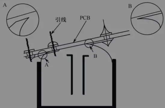
The contact process between the PCB and the wave peak in wave soldering can be roughly divided into three wave zones based on differences in their operational principles, as shown in the diagram below.
1、Wave Entry Point (A)
The initial entry point of the PCB into the wave peak, as shown in the partial enlargement of Point A in the diagram below. Since the PCB moves in the opposite direction to the flow of the solder, the velocity difference at this point is maximum. Therefore, the turbulent flushing action at this point is maximum. This action removes the preheated mixture of flux and rust film residue from the base metal surface to allow direct contact between the solder and the base metal on the PCB. When the wetting temperature is reached, wetting occurs immediately. If the wire surface is coated with a flux protective layer before wave soldering, the turbulent action of the solder fluid will help wash away these surfaces. When the surface is plated with a fusible alloy such as tin-lead solder or pure tin, this principle manifests as a melting-flushing combination effect. For soluble coatings like Ag or Au, this principle manifests as a dissolution-flushing combination effect.
2、Heat Exchange Zone (A-B)
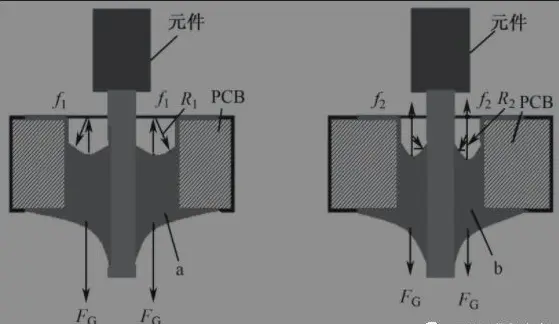
The area where the PCB is immersed in the solder wave peak, as shown in the diagram below between the entry and exit points, is the heat exchange zone. It applies heat and solder to the PCB pads, holes, and component leads. The greater the heat absorption in the welded area, the longer the immersion time in molten solder required to reach the wetting temperature. Therefore, the PCB must be immersed in the solder wave peak for a sufficient duration for the surface energy at the wetting temperature to adsorb the molten solder alloy onto the base metal surface, thereby forming well-filled solder joints.
3、Wave Exit Point (B)
The point where the PCB exits from the solder wave peak, as shown in the partial enlargement on the right (B) in the diagram below, is commonly referred to as the stripping zone. To understand the role of this wave zone, let's briefly analyze the various forces acting on the molten solder filling the solder joints, as shown in the diagram. The surface energy expressed in wetting form will retain the solder in the solder joints, while gravity FG (or the mass of the solder) will try to pull the solder downward. The balance between these forces indicates the necessity of adopting an appropriate ratio of hole diameter to wire diameter, which also depends on solderability. To achieve a balanced state of these forces in the exit zone, the exit point must be located where the solder wave and the PCB are relatively stationary. This can be ensured by matching the speed of the PCB's exit as accurately as possible to the retreating wave speed.
The PCB passes through three wave zones of the solder wave peak:
The forces acting on the liquid solder in the filled solder joint are FG (gravity), f1 and f2 (surface tensions in holes a and b), and R1 and R2 (radii of curvature of the concave surfaces wetted by the solder in holes a and b).
Part I: Formation and Application of the Theory of Wave Soldering Dynamics
Part II: The formation and application of wave soldering wave dynamics theory