 PCB
PCB FPC
FPC Rigid-Flex
 FR-4
FR-4 HDI PCB
 Rogers High-Frequency Board
 PTFE Teflon High-Frequency Board
 Aluminum
 Copper Core
 PCB Assembly
 LED light PCBA
 Memory PCBA
 Power Supply PCBA
 New Energey PCBA
 Communication PCBA
 Industrial Control PCBA
 Medical Equipment PCBA
 Testing Service
 PCBA Testing Service
 Certification Application
 RoHS Certification Application
 REACH Certification Application
 CE Certification Application
 FCC Certification Application
 CQC Certification Application
 UL Certification Application
 Transformers, Inductors
 High Frequency Transformers
 Low Frequency Transformers
 High Power Transformers
 Conversion Transformers
 Sealed Transformers
 Ring Transformers
 Inductors
 Wires,Cables Customized
 Network Cables
 Power Cords
 Antenna Cables
 Coaxial Cables
 Net Position Indicator
 Solar AIS net position indicator
 Capacitors
 Connectors
 Diodes
 Embedded Processors & Controllers
 Digital Signal Processors (DSP/DSC)
 Microcontrollers (MCU/MPU/SOC)
 Programmable Logic Device(CPLD/FPGA)
 Communication Modules/IoT
 Resistors
 Through Hole Resistors
 Resistor Networks, Arrays
 Potentiometers,Variable Resistors
 Aluminum Case,Porcelain Tube Resistance
 Current Sense Resistors,Shunt Resistors
 Switches
 Transistors
 Power Modules
 Isolated Power Modules
 AC-DC Power Modules
 DC-AC Module(Inverter)
 RF and Wireless
Understanding Etch Factor: Calculation Method, Control Targets, and Its Critical Role in PCB Manufacturing
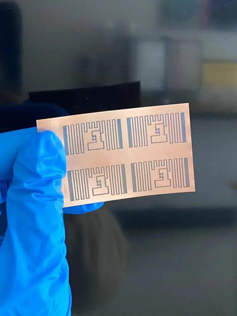
In printed Circuit Board (PCB) fabrication,etchingis a core process for defining conductive traces. The quality of etching directly impacts trace accuracy, impedance consistency, and high-frequency signal integrity. One of the key parameters used to evaluate etching peRFormance is theEtch Factor (EF). This article provides a comprehensive overview of the definition, calculation method, typical control targets, and the impact of etch factor on PCB performance.
1. What Is Etch Factor?
The Etch Factor (EF) is a dimensionless parameter that describes the ratio of the vertical etch depth (i.e., copper thickness) to the horizontal undercut during the etching process. It reflects the degree of anisotropy in the etching—whether the etchant removes material primarily in the vertical direction (ideal) or also erodes laterally beneath the resist mask (undesirable).
In an ideal scenario, etching would be perfectly vertical with zero undercut, resulting in an infinitely high etch factor. In reality, due to the chemical or physical nature of wet or plasma etching, some degree of lateral etching (undercut) always occurs, causing the bottom of the trace to be narrower than the top and forming a trapezoidal cross-section.
2. Calculation Method for Etch Factor
2.1 Basic Formula
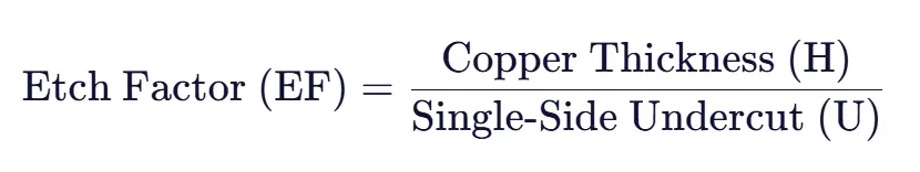
Where:
- H: Copper thickness before etching (in µm or mil), i.e., trace height;
- U: Single-side undercut—the horizontal loss of width on one side of the trace bottom (same units as H).
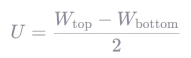
Note: Undercut is typically derived by measuring the top width () and bottom width () of the etched trace:
2.2 Practical Measurement Procedure
- Sampling: Cut a cross-section sample containing representative trace widths from a production panel.
- Sample Preparation: Embed, grind, and polish the sample to create a metallurgical cross-section.
- Microscopy: Capture high-resolution images using an optical microscope or SEM (Scanning Electron Microscope).
- Dimension Measurement:
- Measure copper thickness H;
- Measure top trace width (usually equal to the resist opening);
- Measure bottom trace width .
- Calculation:
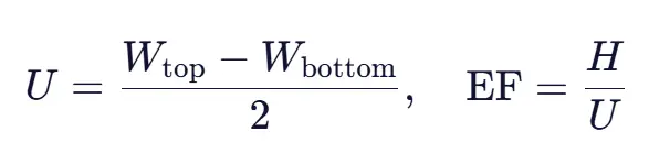
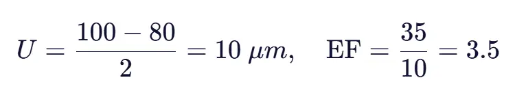
2.3 Example Calculation
Assume:
- Copper thickness (1 oz)
- Top width
- Bottom width
Then:
3. Control Targets for Etch Factor
The etch factor should not be maximized indiscriminately but rather set according to product class, line/space requirements, and signal integrity needs. Industry-standard guidelines are as follows:
| PCB Type | Copper Thickness (H) | Min. Line/Space | Recommended EF | Rationale |
|---|---|---|---|---|
| General Consumer | 18–35 µm | ≥ 0.2 mm | ≥ 2.0 | Basic reliability |
| Mid-to-High-End (Telecom/Industrial) | 35 µm | 0.1–0.15 mm | ≥ 3.0 | Impedance stability |
| High-Speed/High-Frequency (e.g., 5G, Servers) | 12–18 µm (thin copper) | ≤ 0.1 mm | ≥ 4.0 – 5.0 | Minimize skin effect & insertion loss |
| HDI / Fine-Line | ≤ 12 µm | ≤ 50 µm | ≥ 5.0 | Prevent shorts; ensure yield |
Key Principle:
- Finer traces demand higher etch factors (smaller undercut relative to feature size);
- High-frequency designs are sensitive to trace cross-section, as low EF increases conductor resistance and signal loss.
4. Key Factors Influencing Etch Factor
-
Etching Method:
- Acidic etching (e.g., cupric chloride): More isotropic, higher undercut, lower EF (typically 2–3);
- Alkaline etching (e.g., ammoniacal): Better selectivity but still exhibits undercut;
- Plasma etching (dry etch): Highly anisotropic, EF can exceed 10—used in semiconductors but costly for PCBs.
-
Copper Thickness: Thicker copper yields a higher EF for the same undercut, though fine features are harder to achieve.
-
Etchant Parameters:
- Concentration, temperature, spray pressure, and replenishment rate;
- Optimized nozzle design reduces "shadowing" at the trace base, minimizing undercut.
-
Resist Quality:
- Adhesion and edge definition of dry film or ink directly affect etch profile fidelity.
5. Impact of Etch Factor on PCB Performance
- Impedance Control: Low EF reduces effective conductor cross-section, raising characteristic impedance and degrading high-speed signal matching.
- Current Carrying Capacity: Smaller cross-sectional area increases resistive heating.
- Reliability: Severe undercut can cause "necking," leading to trace fracture under thermal cycling.
- Yield: Excessive undercut in fine-pitch designs risks short circuits between adjacent traces.
6. Conclusion
The Etch Factor is a critical metric for assessing PCB etching capability, calculated as EF = Copper Thickness / Single-Side Undercut. Accurate measurement requires cross-sectional analysis via microscopy.
Control targets should be application-driven:
- Standard PCBs: EF ≥ 2.0
- High-speed/high-frequency PCBs: EF ≥ 4.0
- HDI PCBs: EF ≥ 5.0
Achieving high etch factors relies on optimizing etching chemistry, process parameters, copper thickness, and resist performance. As the industry pushes toward higher-density interconnects (HDI) and millimeter-wave frequencies, precise control of etch factor has become an essential capability in advanced PCB manufacturing.