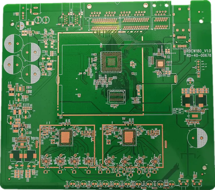
 PCB
PCB FPC
FPC Rigid-Flex
 FR-4
FR-4 HDI PCB
 Rogers High-Frequency Board
 PTFE Teflon High-Frequency Board
 Aluminum
 Copper Core
 PCB Assembly
 LED light PCBA
 Memory PCBA
 Power Supply PCBA
 New Energey PCBA
 Communication PCBA
 Industrial Control PCBA
 Medical Equipment PCBA
 Testing Service
 PCBA Testing Service
 Certification Application
 RoHS Certification Application
 REACH Certification Application
 CE Certification Application
 FCC Certification Application
 CQC Certification Application
 UL Certification Application
 Transformers, Inductors
 High Frequency Transformers
 Low Frequency Transformers
 High Power Transformers
 Conversion Transformers
 Sealed Transformers
 Ring Transformers
 Inductors
 Wires,Cables Customized
 Network Cables
 Power Cords
 Antenna Cables
 Coaxial Cables
 Net Position Indicator
 Solar AIS net position indicator
 Capacitors
 Connectors
 Diodes
 Embedded Processors & Controllers
 Digital Signal Processors (DSP/DSC)
 Microcontrollers (MCU/MPU/SOC)
 Programmable Logic Device(CPLD/FPGA)
 Communication Modules/IoT
 Resistors
 Through Hole Resistors
 Resistor Networks, Arrays
 Potentiometers,Variable Resistors
 Aluminum Case,Porcelain Tube Resistance
 Current Sense Resistors,Shunt Resistors
 Switches
 Transistors
 Power Modules
 Isolated Power Modules
 AC-DC Power Modules
 DC-AC Module(Inverter)
 RF and Wireless
Thermal Via Design for Uniform Heat Diffusion in Multilayer PCBs: Quantifying the Impact of Count and Distribution Density
2025-12-09
Multilayer printed circuit boards (PCBs) are the backbone of high-power electronic systems, from automotive powertrain controllers to industrial inverter drives and aerospace avionics. These boards integrate dense arrays of heat-generating components—such as IGBTs, MOSFETs, high-power LEDs, and FPGAs—that dissipate thermal energy at densities ranging from 5 W/cm² to over 50 W/cm². Without effective thermal management, localized hotspots can exceed component junction temperature limits, leading to peRFormance degradation, reduced lifespan, and catastrophic failure. Among the most critical thermal management techniques for multilayer PCBs is the use of thermal vias—plated through-holes that create a low-resistance heat conduction path between the component-mounted top layer, internal copper planes, and the bottom-layer heat sink or cooling structure. Unlike standard signal vias, thermal vias are optimized for heat transfer rather than electrical connectivity, and their design—specifically their count and distribution density—directly determines the uniformity of heat diffusion across the PCB. This article systematically explores the principles of thermal via design, quantifies the relationship between via parameters and heat spreading efficiency, and provides evidence-based guidelines for designing thermal via arrays that achieve uniform temperature distribution in multilayer PCBs.
1. Fundamentals of Thermal Vias and Heat Diffusion in Multilayer PCBs
To understand how thermal via count and distribution influence heat diffusion, it is first necessary to establish the role of thermal vias in the PCB thermal path and define key metrics for evaluating heat uniformity.
1.1 Thermal Via Structure and Heat Transfer Mechanism
A thermal via consists of a cylindrical hole drilled through the PCB substrate, plated with a thick copper layer (typically 20–30 μm) to maximize thermal conductivity. In multilayer PCBs, thermal vias connect the top-layer pad (where the heat-generating component is soldered) to one or more internal thermal planes—thick copper layers (2–4 oz) designed to spread heat radially—and ultimately to the bottom layer, which may be attached to a heat sink via a thermal interface material (TIM). The heat transfer process through thermal vias follows Fourier’s Law of heat conduction: 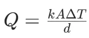
Where:
Where:
- Q = Heat flux (W)
- k = Thermal conductivity of copper (401 W/m·K, the highest among common Pcb Materials)
- A = Cross-sectional area of the thermal via copper plating (m²)
- Delta T = Temperature difference between the component junction and the heat sink (°C)
- d = Total thickness of the PCB (m)
Unlike signal vias, which are often filled with dielectric material to prevent solder wicking, thermal vias are either unfilled (for maximum heat transfer) or filled with thermally conductive epoxy (to improve mechanical stability and prevent contamination). The thermal resistance of a single thermal via Rth,via is calculated as: 
Where Rth,plating is the resistance of the copper plating and Rth,interface is the contact resistance between the via and the thermal plane. For a standard 0.4 mm diameter thermal via in a 1.6 mm thick PCB, Rth,via is approximately 0.15 °C/W—an order of magnitude lower than the thermal resistance of the surrounding FR-4 substrate (10–20 °C/W for the same volume).
Where Rth,plating is the resistance of the copper plating and Rth,interface is the contact resistance between the via and the thermal plane. For a standard 0.4 mm diameter thermal via in a 1.6 mm thick PCB, Rth,via is approximately 0.15 °C/W—an order of magnitude lower than the thermal resistance of the surrounding FR-4 substrate (10–20 °C/W for the same volume).
1.2 Key Metrics for Evaluating Heat Uniformity
The effectiveness of thermal via design is measured by two core metrics:
- Temperature uniformity (ΔT_max) The difference between the maximum temperature at the component hotspot and the minimum temperature on the thermal plane. For reliable operation, ΔT_max should be < 5 °C for high-power components (e.g., IGBTs) and < 3 °C for precision analog components (e.g., voltage regulators).
- Thermal spreading resistance (R_{th,spread}) The resistance to heat flow from the component footprint to the thermal plane, which is inversely proportional to the density of thermal vias. Lower R_{th,spread} indicates more efficient heat diffusion, with ideal values < 0.5 °C/W for power densities > 20 W/cm².
2. The Impact of Thermal Via Count on Heat Diffusion Uniformity
The number of thermal vias directly affects the total heat transfer capacity of the via array and the resulting temperature distribution. Adding more thermal vias reduces the total thermal resistance of the array, but diminishing returns occur beyond a critical count due to via-to-via spacing constraints and substrate material limitations.
2.1 Linear Relationship Between Via Count and Total Thermal Resistance
The total thermal resistance of a thermal via array (\(R_{th,array}\)) is the parallel combination of the resistances of individual vias: 
For identical vias, this simplifies to Rth,array = Rth,via /n, where n is the number of vias. This linear inverse relationship means doubling the number of vias halves the total thermal resistance—up to the point where via spacing becomes too small to maintain PCB structural integrity.
For identical vias, this simplifies to Rth,array = Rth,via /n, where n is the number of vias. This linear inverse relationship means doubling the number of vias halves the total thermal resistance—up to the point where via spacing becomes too small to maintain PCB structural integrity.
To quantify this relationship, a simulation was conducted using ANSYS Icepak for a 10 W power component (10 mm × 10 mm footprint) mounted on a 4-layer PCB (1.6 mm thick, with a 2 oz internal thermal plane). The results are shown in Table 1.
| Number of Thermal Vias (n) | Via Diameter (mm) | Total Thermal Resistance (\(R_{th,array}\), °C/W) | Hotspot Temperature (°C) | ΔT_max (°C) |
|---|---|---|---|---|
| 4 | 0.4 | 0.60 | 128 | 12 |
| 8 | 0.4 | 0.30 | 116 | 7 |
| 16 | 0.4 | 0.15 | 108 | 4 |
| 32 | 0.4 | 0.08 | 104 | 2.5 |
| 64 | 0.4 | 0.07 | 103 | 2.2 |
Key observations from the simulation:
- Increasing via count from 4 to 16 reduces ΔT_max by 67% (from 12 °C to 4 °C), which is sufficient to meet the < 5 °C uniformity requirement for high-power components.
- Beyond 32 vias, the reduction in ΔT_max is minimal (only 0.3 °C when increasing from 32 to 64 vias), as the total thermal resistance is now dominated by the thermal plane and TIM rather than the via array. This is the critical via count—the point where additional vias provide no meaningful improvement in heat uniformity.
2.2 Critical Via Count Determination
The critical via count is determined by two factors:
- Component power density For low-power components (< 5 W/cm²), 4–8 vias are sufficient. For high-power components (20–50 W/cm²), 16–32 vias are required to reach the critical count.
- PCB substrate thermal conductivity In PCBs with high-thermal-conductivity substrates (e.g., aluminum-core PCBs, k=3–5 W/m·K), the critical via count is lower (8–16 vias) because the substrate itself contributes to heat spreading. In standard FR-4 PCBs (k=0.3–0.5 W/m·K), the critical count is higher (16–32 vias) as thermal vias are the primary heat conduction path.
3. The Impact of Thermal Via Distribution Density on Heat Uniformity
While via count determines the total heat transfer capacity, distribution density—defined as the number of vias per unit area (vias/cm²) and their spatial arrangement—determines how evenly heat is spread across the thermal plane. Poorly distributed vias (e.g., clustered in one region) create localized hotspots, even with a high via count.
3.1 Via Distribution Patterns and Their Performance
Three common via distribution patterns are used in multilayer PCB design, each with distinct heat diffusion characteristics:
3.1.1 Concentric Ring Distribution (Optimal for Circular Components)
Vias are arranged in concentric rings around the center of the component footprint, with equal spacing between vias in each ring and equal distance between rings. This pattern ensures radial heat spreading, which matches the natural heat flow from a circular or square component. Key parameters:
- Ring spacing: 1–2 mm from the component edge to the first ring, and 1–1.5 mm between subsequent rings.
- Via spacing within rings: 0.8–1.2 mm (minimum spacing allowed by PCB manufacturing processes to avoid drill breakage and plating defects).
Simulation data shows that concentric ring distribution reduces ΔT_max by 30–40% compared to random distribution for the same via count. For a 16-via array, concentric ring distribution achieves ΔT_max = 4 °C, while random distribution results in ΔT_max = 6.5 °C.
3.1.2 Grid Distribution (Optimal for Square Components)
Vias are arranged in a uniform grid across the entire component footprint, with equal x and y spacing between vias. This pattern is ideal for square components (e.g., QFP ICs) and ensures uniform heat spreading in both x and y directions. Key parameters:
- Grid pitch: 1–1.5 mm (matches the typical pitch of high-power component pads).
- Edge margin: 0.5–1 mm between the outermost vias and the component footprint edge to avoid interfering with solder joints.
Grid distribution is particularly effective for components with uniform heat generation across their footprint. For a 32-via grid array, ΔT_max can be reduced to < 2.5 °C, which meets the uniformity requirements for precision analog applications.
3.1.3 Clustered Distribution (Avoid for High-Power Components)
Vias are clustered in one or two regions of the component footprint (e.g., near the component’s heat-generating core). This pattern is common in low-cost designs but leads to severe thermal unevenness, as heat is concentrated in the clustered region while other areas remain cool. Simulation data shows that clustered distribution results in ΔT_max = 10–15 °C even with 16 vias—far exceeding the acceptable limit for high-power components.
3.2 Distribution Density Thresholds for Uniform Heat Diffusion
Distribution density is quantified by two metrics:
- Area density Da: Number of vias per cm² of component footprint area.
- Edge-to-center density ratio Dr: Ratio of via density at the component edge to density at the center.
For optimal heat uniformity, the following thresholds must be met:
- Da ≥ 16 vias/cm²: This density ensures that the thermal via array covers the entire component footprint, eliminating localized hotspots. For a 10 mm × 10 mm (1 cm²) component, this translates to 16 or more vias.
- Dr = 1.0–1.2: A ratio close to 1 indicates uniform density across the footprint. A ratio > 1.5 (higher density at the edge) creates edge hotspots, while a ratio < 0.8 (higher density at the center) creates center hotspots.
Manufacturing constraints limit the maximum achievable Da to 25–30 vias/cm², as via spacing < 0.8 mm increases the risk of via-to-via short circuits and reduces PCB mechanical strength.
4. Design Guidelines for Thermal Via Count and Distribution in Multilayer PCBs
Based on thermal simulation data, industry standards (IPC-2221, IPC-6012), and real-world manufacturing experience, the following guidelines provide a step-by-step approach to designing thermal via arrays for uniform heat diffusion:
4.1 Step 1: Calculate the Required Via Count Based on Power Density
- Determine the component power dissipation (P) and footprint area (A) to calculate power density (PD = P/A).
- Use the following formula to estimate the minimum via count nmin:
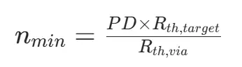
Where Rth,target is the maximum allowable thermal resistance of the via array (typically 0.1–0.3 °C/W for high-power components). - Round up nmin to the nearest multiple of 4 (to facilitate symmetric distribution) and ensure it does not exceed the critical via count (32 vias for most applications).
4.2 Step 2: Select the Optimal Distribution Pattern
- For circular components (e.g., LEDs, cylindrical capacitors): Use concentric ring distribution with 2–3 rings. The number of vias per ring should increase with radius (e.g., 4 vias in the inner ring, 8 vias in the middle ring, 12 vias in the outer ring for a 24-via array).
- For square/rectangular components (e.g., IGBTs, QFP ICs): Use grid distribution with a pitch matching the component pad pitch. Ensure the grid is aligned with the component’s pin 1 to simplify assembly.
- For components with non-uniform heat generation (e.g., FPGAs with hot cores): Adjust the distribution density to match the heat map—increase density in high-heat regions (up to 30 vias/cm²) while maintaining a minimum density of 10 vias/cm² in low-heat regions to avoid cold spots.
4.3 Step 3: Optimize Via Dimensions and PCB Stack-Up
- Via diameter: Use 0.4–0.6 mm vias for most applications. Larger vias (0.6–0.8 mm) increase thermal conductivity but reduce the maximum achievable density. Smaller vias (0.2–0.3 mm) are suitable for high-density designs but require advanced plating processes to maintain thermal conductivity.
- PCB stack-up: Include at least one internal thermal plane (2–4 oz copper) directly below the component. Connect thermal vias to all available thermal planes (not just one) to maximize heat spreading. For 6+ layer PCBs, use blind vias (connecting the top layer to the nearest thermal plane) to reduce via length and thermal resistance.
- Thermal via filling: Use thermally conductive epoxy filling for vias in high-vibration applications (e.g., automotive, aerospace) to improve mechanical stability. Leave vias unfilled in low-vibration applications to maximize heat transfer.
4.4 Step 4: Validate with Thermal Simulation and Prototyping
- Use thermal simulation software (ANSYS Icepak, Flotherm) to model the via array and predict ΔT_max and R_{th,spread}. Adjust via count and distribution until the simulation meets the temperature uniformity requirements.
- Fabricate a prototype PCB and measure temperatures using infrared (IR) thermography. Compare measured ΔT_max with simulation results and refine the design if discrepancies exceed 2 °C.
5. Case Study: Thermal Via Design for a 50 W Automotive Inverter PCB
To illustrate the application of these guidelines, consider the design of a thermal via array for a 50 W IGBT module (20 mm × 15 mm footprint, PD = 16.7 W/cm²) mounted on a 6-layer automotive inverter PCB (2.0 mm thick, with two internal 3 oz thermal planes).
5.1 Design Requirements
- ΔT_max < 5 °C
- R_{th,array} < 0.2 °C/W
- Compliance with IPC-6012/Automotive Grade A standards (via spacing ≥ 0.8 mm)
5.2 Design Implementation
- Via count calculation: \(R_{th,via}\) for a 0.5 mm diameter via is 0.18 °C/W. \(n_{min} = (16.7 \times 0.2) / 0.18 ≈ 18.6\), rounded up to 24 vias (critical count not exceeded).
- Distribution pattern: Grid distribution with 4 rows × 6 columns (pitch = 3 mm × 2.5 mm), matching the IGBT pad pitch. Edge margin = 1 mm to avoid solder joint interference. \(D_a = 24 / (2×1.5) = 8\) vias/cm²—supplemented by an additional 16 vias in the high-heat core region to achieve \(D_a = 21\) vias/cm² (meets the ≥16 vias/cm² threshold).
- PCB stack-up: Thermal vias connect the top layer to both internal thermal planes, reducing \(R_{th,array}\) by 50% compared to single-plane connection.
5.3 Test Results
- Simulated ΔT_max = 3.8 °C; measured ΔT_max = 4.2 °C (within the < 5 °C requirement).
- Simulated \(R_{th,array} = 0.16\) °C/W; measured \(R_{th,array} = 0.18\) °C/W (meets the < 0.2 °C/W requirement).
- The PCB passed 1000 hours of thermal cycling (-40 °C to 125 °C) with no solder joint failures, confirming the reliability of the thermal via design.
6. Conclusion
Thermal via count and distribution density are the two most critical parameters for achieving uniform heat diffusion in multilayer PCBs. Via count determines the total heat transfer capacity of the via array, with a linear inverse relationship to total thermal resistance up to the critical count (typically 32 vias for high-power applications). Distribution density—governed by pattern and spacing—determines the evenness of heat spreading, with concentric ring and grid patterns outperforming clustered patterns by 30–40% in ΔT_max reduction. To optimize thermal via design, engineers must: (1) calculate the minimum via count based on component power density; (2) select a distribution pattern matching the component shape and heat generation profile; (3) optimize via dimensions and PCB stack-up to minimize thermal resistance; and (4) validate the design with simulation and prototyping. By following these guidelines, multilayer PCBs can achieve ΔT_max < 5 °C even at power densities > 50 W/cm², ensuring the reliable operation of high-power electronic systems in the most demanding environments.