 PCB
PCB FPC
FPC Rigid-Flex
 FR-4
FR-4 HDI PCB
 Rogers High-Frequency Board
 PTFE Teflon High-Frequency Board
 Aluminum
 Copper Core
 PCB Assembly
 LED light PCBA
 Memory PCBA
 Power Supply PCBA
 New Energey PCBA
 Communication PCBA
 Industrial Control PCBA
 Medical Equipment PCBA
 Testing Service
 PCBA Testing Service
 Certification Application
 RoHS Certification Application
 REACH Certification Application
 CE Certification Application
 FCC Certification Application
 CQC Certification Application
 UL Certification Application
 Transformers, Inductors
 High Frequency Transformers
 Low Frequency Transformers
 High Power Transformers
 Conversion Transformers
 Sealed Transformers
 Ring Transformers
 Inductors
 Wires,Cables Customized
 Network Cables
 Power Cords
 Antenna Cables
 Coaxial Cables
 Net Position Indicator
 Solar AIS net position indicator
 Capacitors
 Connectors
 Diodes
 Embedded Processors & Controllers
 Digital Signal Processors (DSP/DSC)
 Microcontrollers (MCU/MPU/SOC)
 Programmable Logic Device(CPLD/FPGA)
 Communication Modules/IoT
 Resistors
 Through Hole Resistors
 Resistor Networks, Arrays
 Potentiometers,Variable Resistors
 Aluminum Case,Porcelain Tube Resistance
 Current Sense Resistors,Shunt Resistors
 Switches
 Transistors
 Power Modules
 Isolated Power Modules
 AC-DC Power Modules
 DC-AC Module(Inverter)
 RF and Wireless
The Role of C-SAM in SMT Process Analysis
The Role of C-SAM in SMT Process Analysis
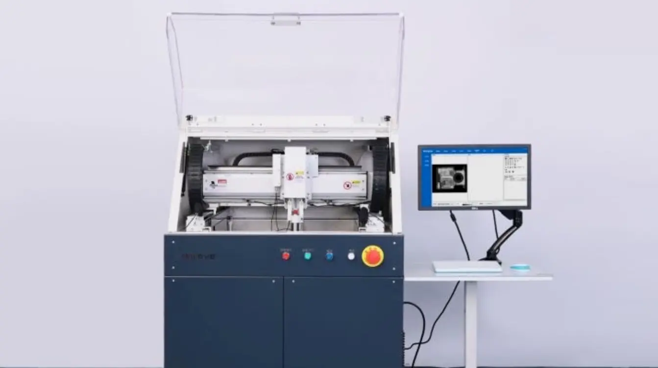
1. Basic Understanding of C-SAM Technology
C-SAM, or Confocal Scanning Acoustic Microscopy, is an advanced non-destructive testing technology. Its working principle is based on the propagation characteristics of ultrasonic waves in different media. When ultrasonic waves propagate inside a material, they encounter inteRFaces with different physical properties such as density and elastic coefficients, resulting in reflection and transmission. C-SAM utilizes this characteristic by emitting and receiving ultrasonic waves and analyzing the echoes to detect internal structures and defects within materials.
C-SAM technology has several notable features:
-
Non-destructive testing: It does not damage the object being tested, which is particularly important for precious or irreparable samples.
-
High precision: It can detect defects at the micron or even sub-micron level, identifying tiny defects and structural anomalies.
-
Versatility: It can detect various types of defects, such as delamination, cracks, and voids, making it widely applicable.
-
Non-contact detection: It avoids potential contamination or damage to the sample during the testing process.
2. Key Applications of C-SAM in SMT Processes
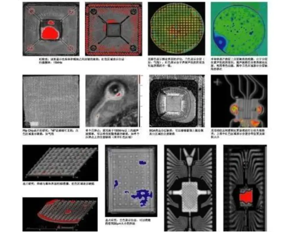
(1) Electronic Components
In SMT (Surface Mount Technology) processes, the quality of electronic components is crucial. C-SAM can be used to detect internal defects such as delamination, cracks, and voids in electronic components. High-frequency ultrasonic scanning can precisely capture these small but potentially performance-affecting defects. For example, in integrated circuits, C-SAM can detect structural anomalies within the chip, ensuring its stability and reliability during operation.
(2) LEDs
C-SAM plays a critical role in the SMT assembly of LED products. It can effectively detect issues such as delamination in LED packaging, cracks between the chip and substrate, and potential voids. If these defects are not identified in time, they can lead to uneven light emission, reduced brightness, or complete failure of the LED.
(3) Metal Substrates
Metal substrates are commonly used in SMT to carry electronic components. C-SAM can detect defects such as delamination in the substrate's coating, internal cracks, and voids. These defects, which may arise during manufacturing or use, can affect the substrate's thermal and electrical conductivity, thereby impacting the stability of the entire electronic device.
In summary, C-SAM's ability to detect defects in electronic components, LEDs, and metal substrates in SMT processes significantly improves product quality, reduces waste, and supports the high-quality development of the electronics manufacturing industry.
3. Advantages of C-SAM in SMT Processes
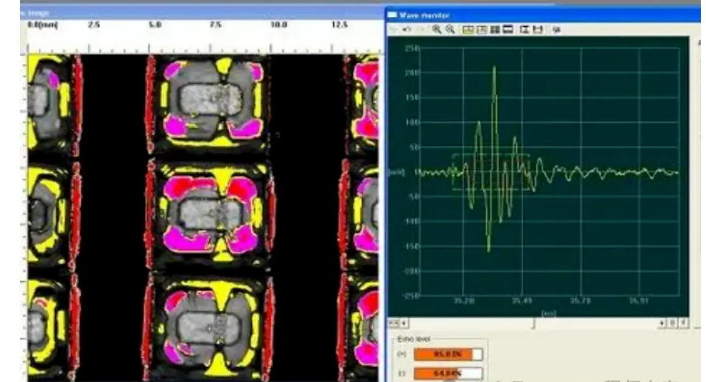
(1) Precise Defect Localization
C-SAM can accurately determine the specific layer where a defect is located, a significant advantage over many other testing technologies. For example, while X-ray testing can identify defects, it often cannot pinpoint the exact layer. C-SAM, however, can clearly show the depth and position of defects within the material, providing targeted guidance for subsequent repairs and improvements.
(2) Sensitive Detection of Flat Interface Discontinuities
C-SAM is highly sensitive to discontinuities in flat interfaces. Compared to other testing methods that might miss or misjudge such subtle defects, C-SAM can effectively detect small cracks and gaps, greatly enhancing the accuracy and reliability of testing.
(3) Superior Analysis of Internal Delamination in Plastic-Encapsulated Devices
C-SAM excels in analyzing internal delamination in plastic-encapsulated devices. It can clearly reveal the location, extent, and severity of delamination, whereas other testing technologies often struggle with such issues.
In conclusion, these advantages make C-SAM an indispensable tool in SMT processes, effectively ensuring product quality, reducing defect rates, and improving production efficiency.
4. Case Studies
(1) Failure Analysis of Surface-Mount MOSFET Products
In the production of surface-mount MOSFET products, it is common for products that pass electrical parameter tests to fail after SMT assembly, with issues such as leakage between the drain and source (D, S) or short circuits. The failure rate can exceed 50%. Analysis suggests that due to the large chip area and specific surface-mount packaging, stress matching issues often arise during assembly, especially under high humidity and airtightness requirements.
In this case, C-SAM was used to scan for delamination in products subjected to simulated SMT conditions. Ultrasonic scanning revealed severe delamination between the product's pad area (PAD) and the molding compound. Further dissection of the failed products showed internal cracks in the chips. This case highlights C-SAM's accuracy and effectiveness in detecting delamination and internal cracks in surface-mount MOSFET products. By identifying these issues early, manufacturers can improve packaging processes, select more suitable materials, and optimize production, thereby reducing failure rates and ensuring product quality and reliability.
(2) Other Cases
Beyond MOSFET failure analysis, C-SAM has been successfully applied in various SMT processes involving electronic components, LEDs, and metal substrates. For example:
-
In electronic component production, C-SAM detected minor delamination within chips, allowing manufacturers to adjust processes and avoid potential quality issues.
-
In LED assembly, C-SAM accurately identified cracks between chips and substrates, enabling the screening and repair of defective products and improving yield rates.
-
For metal substrates, C-SAM detected coating delamination and internal cracks, helping manufacturers optimize substrate production and enhance performance and stability.
These cases further demonstrate the significant role and broad application value of C-SAM in SMT processes.