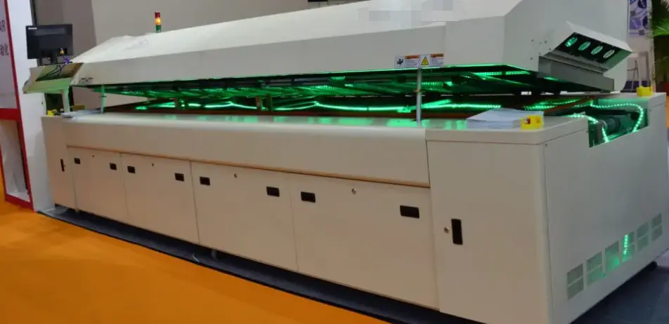
The reflow oven is the core equipment for SMT soldering, and its working status directly determines the melting, wetting, and solidifICation processes of solder. The essence of daily maintenance is to eliminate equipment anomalies (such as contaminant accumulation and temperature deviations) and ensure the internal oven environment stably meets soldering process requirements (e.g., temperature profile, conveyor stability). Neglecting maintenance will lead to numerous soldering defects (e.g., cold joints, over-soldering, component damage) due to equipment deterioration—even if soldering parameters are set correctly. Industry statistics show that approximately 30% of SMT soldering defects result from improper reflow oven maintenance, making daily maintenance an "invisible defense line" for ensuring soldering quality. Daily cleaning of the conveyor belt (typically stainless steel mesh or Teflon-coated mesh) is required:
- After soldering, use a dedicated plastic scraper (to avoid scratching the belt) to remove residual solder balls and flux (flux residue buildup) from the suRFace;
- Weekly, soak belt joints and mesh gaps in an ultrasonic cleaner (with neutral detergent) to remove stubborn flux residues;
- Monthly, check belt tension (adjust the tension pulley if loose) and surface flatness (replace local sections if deformed or damaged).
- Solder Residue and Flux Buildup: Solder balls on the belt surface will "elevate" the PCB during conveyance, causing uneven hot air contact (local insufficient temperature) and cold joints (solder fails to fully wet leads). Flux buildup will adhere to the PCB bottom, leading to conveyance deviation (e.g., PCB tilting) and solder joint misalignment (solder deviates from pads, even shorting adjacent pins).
- Belt Deformation and Insufficient Tension: A loose belt causes fluctuating PCB conveyance speed (fast-slow cycles), making the PCB’s residence time in each temperature zone deviate from settings—e.g., insufficient preheating time (flux not fully activated) leads to pinholes (incomplete flux volatilization in the soldering zone). Local belt bulging scratches the PCB, causing component displacement (e.g., 0402 chip Resistor offset) and false joints (only partial solder contacts leads).
A cleaned belt ensures stable PCB conveyance (deviation ≤0.1mm) with ≥95% removal of solder/flux residues, reducing cold joint and misalignment defects by over 60%. Regular tension adjustment controls conveyance speed error within ±1%, ensuring temperature profile stability.
Weekly temperature calibration is required, adhering to IPC-TM-650 2.4.13:
- Use a temperature profiler (e.g., KIC 2000) to attach thermocouple probes to critical PCB locations (e.g., BGA center, 01005 component pad, PCB edge) and run one simulation of the actual production process;
- Compare the test profile with the set profile (e.g., "preheat→soak→reflow→cool" for lead-free soldering). If any zone deviates by >3℃ (e.g., set reflow peak 250℃ vs. actual 246℃), adjust the corresponding heater power;
- Monthly calibrate thermocouple sensors (replace aged probes); quarterly, invite third-party institutions to test internal temperature uniformity (requiring ≤5℃ difference between any two points).
- Insufficient Temperature (Cold Soldering Risk): Inadequate preheating temperature (e.g., set 150℃ vs. actual 140℃) prevents flux from removing oxide layers, causing cold joints (dull, low-strength solder joints prone to peeling). Insufficient reflow peak temperature (e.g., lead-free solder melting point 217℃ vs. actual 210℃) results in partial melting (paste-like solder failing to wrap leads).
- Excessive Temperature (Over-Soldering Risk): Over 260℃ in the reflow zone causes excessive solder oxidation (SnO₂ formation), leading to solder voids (oxide layers block solder flow, creating bubbles). High temperatures also damage components (e.g., plastic IC deformation, MLCC cracking) or cause PCB discoloration/delamination (resin decomposition), reducing circuit reliability.
- Temperature Inhomogeneity (Poor Consistency): >8℃ internal temperature variation (e.g., 250℃ left vs. 242℃ right) causes "some cold joints, some over-soldering" in the same PCB batch, with >15% yield fluctuation, failing to ensure mass production stability.
Post-calibration, each zone’s deviation is controlled within ±2℃, temperature uniformity ≤4℃, and cold/over-soldering defects decrease by over 80%. The pass rate of critical components (e.g., BGA, QFP) rises to >99.5%, meeting IPC-A-610 Class 2 requirements.
Biweekly cleaning of heating elements and the hot air system is required:
- After powering off and cooling to room temperature, open the oven chamber cover and use compressed air (0.5MPa) to blow off flux dust from heating elements (preventing insulating dust buildup);
- Wipe hot air fan blades with alcohol swabs (removing oil/dust) and check for bearing noise (add lubricant if needed);
- Monthly inspect heating elements for damage (e.g., local blackening, deformation). Replace elements with >20% power attenuation to avoid affecting zone temperatures.
- Heating Element Scaling (Reduced Efficiency): >0.5mm flux dust buildup on elements reduces heat transfer by 30%, preventing temperature zones from reaching set values—e.g., scaled preheating elements lower PCB heating rate from 3℃/min to 1.5℃/min, causing solder splattering (volatilized gas impacts molten solder).
- Hot Air Fan Dust (Airflow Turbulence): Dust on fan blades disrupts hot air circulation (local wind speed drops from 1.5m/s to 0.8m/s), creating "hot spots" (over-soldering) and "cold spots" (cold joints) on PCBs. This significantly affects fine-pitch components (e.g., 0.3mm QFP), leading to pin bridging.
Cleaned elements restore heat transfer efficiency to >95%, hot air speed fluctuation ≤0.2m/s, and PCB heating rate deviation ≤±0.5℃/min, reducing local insufficient heating defects by 70%.
Monthly maintenance of the cooling system (typically forced air or water cooling) is required:
- Air cooling: Clean the fan filter (removing dust to avoid blocked ventilation) and check fan speed (replace if <80% of rated speed);
- Water cooling: Inspect for pipe leaks, replace coolant every 6 months (preventing scale blockage), and ensure outlet temperature ≤50℃ (clean the heat exchanger if exceeded).
- Insufficient Cooling (Slow Solidification): Cooling rate <5-8℃/s (e.g., >60s to cool from 220℃ to 100℃ vs. standard ≤40s) prolongs solder solidification, causing coarse grain growth (loose joint microstructure) and reduced mechanical strength (20-30% lower tensile strength, prone to vibration-induced fracture). Slow cooling also causes excessive intermetallic compound (e.g., Cu₃Sn) formation, reducing conductivity.
- Uneven Cooling (Uneven Joint Stress): Local cooling system blockage causes uneven PCB cooling rates (fast edges, slow center), generating thermal stress and solder joint cracks (especially invisible BGA ball cracks, leading to later failure).
Maintained cooling systems achieve stable 5-8℃/s cooling rates, ≤3℃ uniformity, refined solder grains, and >95% of standard tensile strength, reducing thermal stress cracks by 90%.
For nitrogen-protected reflow ovens (used for lead-free or high-reliability products), monthly maintenance is required:
- Check nitrogen generator purity (require O₂ content ≤50ppm via oxygen analyzer) and replace molecular sieves if purity is insufficient;
- Clean nitrogen nozzles (prevent blockage-induced uneven distribution) and ensure stable flow (e.g., 10-15L/min).
Neglecting this system causes excessive oxygen (>100ppm), 加剧 solder oxidation, and leads to dull joints and pinholes—especially damaging to enclosed joints (e.g., BGA). Maintenance controls oxygen content ≤30ppm, reducing oxidation defects by 85%.
Implementation note: After maintenance, conduct a "pilot production verification" (soldering 50-100 PCBs) to test yield and joint quality before resuming mass production. Maintain a maintenance log to record timing, content, and test results for traceability.
 PCB
PCB FPC
FPC Rigid-Flex
 FR-4
FR-4 HDI PCB
 Rogers High-Frequency Board
 PTFE Teflon High-Frequency Board
 Aluminum
 Copper Core
 PCB Assembly
 LED light PCBA
 Memory PCBA
 Power Supply PCBA
 New Energey PCBA
 Communication PCBA
 Industrial Control PCBA
 Medical Equipment PCBA
 Testing Service
 PCBA Testing Service
 Certification Application
 RoHS Certification Application
 REACH Certification Application
 CE Certification Application
 FCC Certification Application
 CQC Certification Application
 UL Certification Application
 Transformers, Inductors
 High Frequency Transformers
 Low Frequency Transformers
 High Power Transformers
 Conversion Transformers
 Sealed Transformers
 Ring Transformers
 Inductors
 Wires,Cables Customized
 Network Cables
 Power Cords
 Antenna Cables
 Coaxial Cables
 Net Position Indicator
 Solar AIS net position indicator
 Digital Signal Processors (DSP/DSC)
 Microcontrollers (MCU/MPU/SOC)
 Programmable Logic Device(CPLD/FPGA)
 Through Hole Resistors
 Resistor Networks, Arrays
 Potentiometers,Variable Resistors
 Aluminum Case,Porcelain Tube Resistance
 Current Sense Resistors,Shunt Resistors
 Isolated Power Modules
 AC-DC Power Modules
 DC-AC Module(Inverter)
 Capacitors
  Connectors
  Diodes
 Embedded Processors & Controllers
 Communication Modules/IoT
 Resistors
 Switches
 Transistors
 Power Modules
 RF and Wireless