 PCB
PCB FPC
FPC Rigid-Flex
 FR-4
FR-4 HDI PCB
 Rogers High-Frequency Board
 PTFE Teflon High-Frequency Board
 Aluminum
 Copper Core
 PCB Assembly
 LED light PCBA
 Memory PCBA
 Power Supply PCBA
 New Energey PCBA
 Communication PCBA
 Industrial Control PCBA
 Medical Equipment PCBA
 Testing Service
 PCBA Testing Service
 Certification Application
 RoHS Certification Application
 REACH Certification Application
 CE Certification Application
 FCC Certification Application
 CQC Certification Application
 UL Certification Application
 Transformers, Inductors
 High Frequency Transformers
 Low Frequency Transformers
 High Power Transformers
 Conversion Transformers
 Sealed Transformers
 Ring Transformers
 Inductors
 Wires,Cables Customized
 Network Cables
 Power Cords
 Antenna Cables
 Coaxial Cables
 Net Position Indicator
 Solar AIS net position indicator
 Capacitors
 Connectors
 Diodes
 Embedded Processors & Controllers
 Digital Signal Processors (DSP/DSC)
 Microcontrollers (MCU/MPU/SOC)
 Programmable Logic Device(CPLD/FPGA)
 Communication Modules/IoT
 Resistors
 Through Hole Resistors
 Resistor Networks, Arrays
 Potentiometers,Variable Resistors
 Aluminum Case,Porcelain Tube Resistance
 Current Sense Resistors,Shunt Resistors
 Switches
 Transistors
 Power Modules
 Isolated Power Modules
 AC-DC Power Modules
 DC-AC Module(Inverter)
 RF and Wireless
Part II: The formation and application of wave soldering wave dynamics theory
Part II: The formation and applICation of wave soldering wave dynamics theory
III. The influence of wave velocity of wave soldering on the effect of wave soldering
As discussed in the dynamic phenomenon of solder wave, when the PCB enters the working range of the wave, there is a boundary layer near the lower suRFace of the PCB due to the opposite direction of motion of the PCB and the flow direction of the liquid solder. The thickness of the boundary layer is related to the pinching speed of the PCB and the fluid flow rate in the direction opposite to the PCB's motion. For example, when the pinching speed of the PCB is constant, increasing the reverse fluid flow speed will reduce the thickness of the boundary layer, significantly weaken the backflow phenomenon, and significantly enhance the reverse scrubbing effect of the solder fluid on the PCB. Obviously, it is not easy to produce the phenomenon of tipping and bridging, but it is likely that the amount of solder required for forming the normal outline of the solder joint will also be excessively scrubbed away, resulting in defects such as insufficient tin intake, dryness, and asymmetric outline of the solder joint. On the contrary, if the fluid velocity is too low, the scrubbing effect will be reduced, and the solder joints will be fuller, but the probability of producing tipping and bridging will also increase. Therefore, for a specific PCB and its pinching speed, there is an optimal liquid solder fluid speed. The following figure shows a typical solder wave shape and its flow rate adjustment structure.
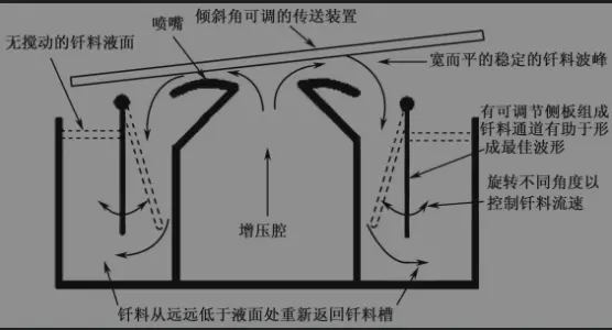
In the above figure, a large pressurized cavity is used to press the molten solder into the nozzle, and a smooth laminar bidirectional flow is obtained through the nozzle. The liquid solder flow passes through the nozzle flange to form a solder wave crest. The nozzle shape controls the shape of the solder wave crest, and therefore also controls the role of wave crest dynamics. A buffer net is installed within the pressure chamber to ensure the formation of laminar flow, thereby ensuring the smoothness of the wave crest. To reduce the generation of solder slag, the solder pouring down from the peak should not have excessive turbulence when returning to the solder tank. The adjustable side plates, positioned on the front and rear outer sides of the nozzle, constitute the solder reflow channel and aid in creating the optimal wave peak. They force the solder from the wave peak to return to the solder tank from a position significantly below the liquid level, thereby maintaining the liquid level in the solder tank undisturbed. By adjusting the inclination angle of the side plate, the flow of the solder can be controlled by gradually decelerating as it returns to the solder tank along the inclined surface, thereby minimizing surface turbulence. By adjusting the side plate located in front of the nozzle, the shape of the wave crest entering the working area can be controlled, thereby controlling the velocity characteristics of the fluid in this area. Similarly, there is also a problem of matching the PCB transfer speed with the fluid speed in the PCB exit section to obtain the best separation conditions. At this time, it can be achieved by adjusting the side plate located behind the nozzle.
IV.Fourth, the types and characteristics of solder wave peaks
There are many types of wave soldering equipment currently operating in industrial production, and these devices can be roughly divided into the following two categories based on the type of waveform.
1、 One-way wave crest type This type of nozzle wave crest solder flow structure is more common in early equipment. Now, except for hollow wave, other unidirectional waveforms are not common on newer machines.
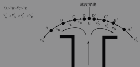
2、 Bidirectional wave peak system The characteristic of this bidirectional wave peak system is that the liquid solder coming out of the nozzle flows in both directions, forward and backward, after reaching the top of the nozzle. According to the needs of the application, this shunt can be symmetrical or asymmetrical, and even an extender is added along the backward direction of the transmission to make the wave peak wider and flatter in the direction of PCB dragging. At present, the most commonly used wave soldering equipment is the two-way wave type. Due to the distribution characteristics of the surface velocity of the wave peak, the bidirectional wave peak system can minimize the problem of solder joint tapering. Due to the flow of solder in the front and rear directions in the solder wave, there must be a region with zero velocity on the surface of the solder wave. The PCB exits near the area where the speed is zero, as shown in the figure below, which is crucial for the formation of solder joints without a pull-up.
Part I: Formation and Application of the Theory of Wave Soldering Dynamics