 PCB
PCB FPC
FPC Rigid-Flex
 FR-4
FR-4 HDI PCB
 Rogers High-Frequency Board
 PTFE Teflon High-Frequency Board
 Aluminum
 Copper Core
 PCB Assembly
 LED light PCBA
 Memory PCBA
 Power Supply PCBA
 New Energey PCBA
 Communication PCBA
 Industrial Control PCBA
 Medical Equipment PCBA
 Testing Service
 PCBA Testing Service
 Certification Application
 RoHS Certification Application
 REACH Certification Application
 CE Certification Application
 FCC Certification Application
 CQC Certification Application
 UL Certification Application
 Transformers, Inductors
 High Frequency Transformers
 Low Frequency Transformers
 High Power Transformers
 Conversion Transformers
 Sealed Transformers
 Ring Transformers
 Inductors
 Wires,Cables Customized
 Network Cables
 Power Cords
 Antenna Cables
 Coaxial Cables
 Net Position Indicator
 Solar AIS net position indicator
 Capacitors
 Connectors
 Diodes
 Embedded Processors & Controllers
 Digital Signal Processors (DSP/DSC)
 Microcontrollers (MCU/MPU/SOC)
 Programmable Logic Device(CPLD/FPGA)
 Communication Modules/IoT
 Resistors
 Through Hole Resistors
 Resistor Networks, Arrays
 Potentiometers,Variable Resistors
 Aluminum Case,Porcelain Tube Resistance
 Current Sense Resistors,Shunt Resistors
 Switches
 Transistors
 Power Modules
 Isolated Power Modules
 AC-DC Power Modules
 DC-AC Module(Inverter)
 RF and Wireless
The Critical Threshold in Buried Via Design: How an 8:1 Aspect Ratio Drops Plating Yield Below 90%
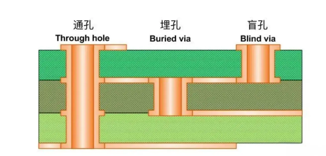
In buried via design, the critICal aspect ratio (ratio of via depth to diameter) that typically leads to a drop in copper plating yield below 90% is around 8:1. When the aspect ratio exceeds this threshold, achieving reliable and uniform copper deposition becomes significantly more challenging, often requiring specialized processes to maintain acceptable quality.
Here is a table summarizing the general relationship between aspect ratio and plating peRFormance for reference:
| Aspect Ratio | Plating Performance & Typical Process | Key Challenges |
|---|---|---|
| ≤ 6:1 | Reliable plating, uniform copper deposition. Standard processes often suffice. | Standard process control. |
| > 6:1 to 8:1 | Increasing risk of plating defects. May require process adjustments. | Ensuring complete via filling, avoiding voids. |
| ≥ 8:1 | Significant yield challenge. Copper plating yield can drop below 90%. Specialized processes needed. | Inadequate copper deposition in the center, leading to voids or discontinuous plating. |
🔍 Understanding the Impact of High Aspect Ratios
A high aspect ratio in a buried via means the hole is relatively deep and narrow. This geometry creates several physical challenges that hinder the copper plating process, which is essential for creating a reliable electrical connection between internal layers of the PCB.
-
Impaired Solution Flow and Ion Transport: During the chemical copper deposition (electroless copper) process, the plating solution must flow freely through the via to replenish copper ions. In high-aspect-ratio vias, this solution exchange is severely restricted. The result is a depletion of copper ions in the center of the via, leading to thin or non-existent copper plating in that area.
-
Difficulty in Air Bubble Removal: Air bubbles trapped during the wet chemical processing steps can be difficult to dislodge from deep, narrow vias. These bubbles block the plating solution from contacting the hole wall, creating voids in the final copper layer.
-
Limitations of Electroplating: Even if a initial conductive layer is successfully deposited, subsequent electroplating steps struggle with high aspect ratios. The "throwing power" of the electroplating solution—its ability to deposit metal uniformly in deep recesses—is limited. This often results in a phenomenon where the mouth of the via is over-plated while the center remains poorly plated, potentially leading to a closed via mouth and an internal defect.
🛠️ Process Strategies for Challenging Aspect Ratios
When the design requires aspect ratios that push the limits of standard processes, manufacturers employ several advanced techniques to mitigate risks and improve yields.
-
Specialized Plating Processes: For demanding applications, pulse plating can be more effective than traditional DC plating. Pulse plating alternates the current in precise cycles, which helps replenish copper ions within the via and improves the uniformity of the deposition.
-
Process and Equipment Enhancements: SIMple mechanical improvements can make a big difference. Adding agitation or vibration to the plating tanks helps force fresh solution into high-aspect-ratio vias and assists in dislodging trapped air bubbles. Furthermore, adjusting the chemistry of the plating bath, such as increasing the sulfuric acid-to-copper sulfate ratio, can enhance the solution's throwing power for deeper penetration.
-
Alternative Filling Methods: For buried vias with an aspect ratio greater than 6:1, a plugging plating process might be necessary instead of a simple through-hole plating process to ensure the via is filled and the copper thickness meets requirements.
💡 Design for Manufacturing (DFM) Advice
To ensure high yield and reliability, consider these principles during the design phase:
-
Control the Aspect Ratio: Whenever possible, aim for an aspect ratio of 8:1 or lower for buried vias to maintain a high copper plating yield. This is the most straightforward way to avoid process-related defects.
-
Prioritize Larger Diameters: If increasing the depth is unavoidable, see if you can also increase the via diameter to keep the aspect ratio manageable. For critical current-carrying vias, prioritize a diameter of 0.5mm or larger (aspect ratio ≤5:1)
-
Communicate with Your Manufacturer: Early consultation with your PCB fabricator is vital. Discuss your design constraints and their specific process capabilities for high-aspect-ratio vias. They can provide tailored guidelines on the aspect ratios their production line can reliably handle.
-
Leverage DFM Analysis: Before releasing your design for production, use DFM software to run a comprehensive check. These tools can automatically flag features like high-aspect-ratio vias that are at risk of manufacturing failures.
✅ Conclusion
In summary, the aspect ratio of a buried via is a critical parameter that directly impacts the success of the copper plating process. While standard processes work well for ratios up to 6:1, a ratio of 8:1 is a critical threshold, beyond which the copper plating yield is likely to fall below 90%. By understanding the physical challenges, being aware of advanced manufacturing techniques, and adhering to DFM principles, you can design buried vias that are both high-performing and manufacturable.