 PCB
PCB FPC
FPC Rigid-Flex
 FR-4
FR-4 HDI PCB
 Rogers High-Frequency Board
 PTFE Teflon High-Frequency Board
 Aluminum
 Copper Core
 PCB Assembly
 LED light PCBA
 Memory PCBA
 Power Supply PCBA
 New Energey PCBA
 Communication PCBA
 Industrial Control PCBA
 Medical Equipment PCBA
 Testing Service
 PCBA Testing Service
 Certification Application
 RoHS Certification Application
 REACH Certification Application
 CE Certification Application
 FCC Certification Application
 CQC Certification Application
 UL Certification Application
 Transformers, Inductors
 High Frequency Transformers
 Low Frequency Transformers
 High Power Transformers
 Conversion Transformers
 Sealed Transformers
 Ring Transformers
 Inductors
 Wires,Cables Customized
 Network Cables
 Power Cords
 Antenna Cables
 Coaxial Cables
 Net Position Indicator
 Solar AIS net position indicator
 Capacitors
 Connectors
 Diodes
 Embedded Processors & Controllers
 Digital Signal Processors (DSP/DSC)
 Microcontrollers (MCU/MPU/SOC)
 Programmable Logic Device(CPLD/FPGA)
 Communication Modules/IoT
 Resistors
 Through Hole Resistors
 Resistor Networks, Arrays
 Potentiometers,Variable Resistors
 Aluminum Case,Porcelain Tube Resistance
 Current Sense Resistors,Shunt Resistors
 Switches
 Transistors
 Power Modules
 Isolated Power Modules
 AC-DC Power Modules
 DC-AC Module(Inverter)
 RF and Wireless
Suppressing Simultaneous Switching Noise Using Electromagnetic Bandgap (EBG) Structures
2025-07-08
1. SSN Mechanism & EBG Principle
-
SSN Generation:
-
: P/G loop inductance (0.5-2nH)
-
: Simultaneously Switching gates
-
: Current slew rate (up to 1A/ns)
-
-
EBG Bandgap Property:
Frequency Attenuation Mechanism Suppression In-band (e.g., 1-5GHz) Propagation prohibition >40dB Out-of-band Partial reflection/absorption <10dB
2. EBG Topologies & Design
2.1 Topology Comparison
| Type | Structure | Band (GHz) | Process Complexity |
|---|---|---|---|
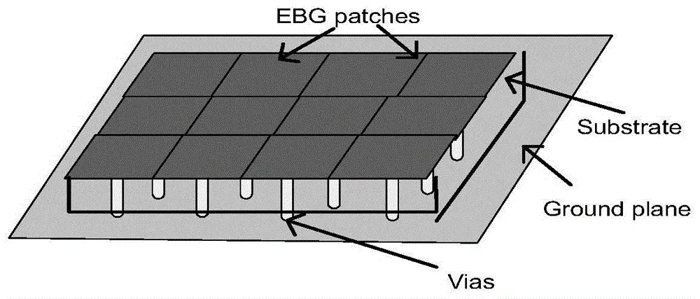
| Mushroom | Metal patch + vertICal via | 0.5-10 | High |
| Planar | Periodic slots/patches | 2-20 | Medium |
| HIS (High-Impedance Surface) | LC resonator array | 1-6 | Low |
2.2 Key Design Formulas
-
Center Frequency:
-
Bandwidth:
3. Design Optimization Flow
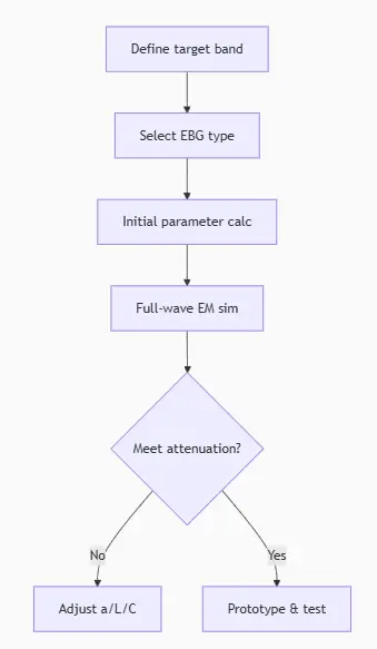
3.1 Parameter Tuning
| Variable | Adjustment | Bandgap Impact |
|---|---|---|
| Unit period a | ↑ | ↓, BW↓ |
| Patch size | ↑ | ↓, BW↑ |
| Dielectric thickness h | ↑ | ↓, BW↑ |
| Via diameter d | ↑ | ↑, BW↓ |
4. PCB Implementation
| Integration | Structure | SSN Suppression | Cost |
|---|---|---|---|
| P/G layer EBG | Replace partial ground plane | 30-45dB | +2-4 layers |
| Local EBG island | 5×5 array under critical ICs | 20-30dB | 10% routing area |
| Edge EBG fence | Perimeter EBG (width≥λ/4) | 15-25dB | +5% board size |
5. Performance Validation
5.1 Simulation
| Software | Key Settings | Accuracy |
|---|---|---|
| HFSS | Sweep DC-20GHz, mesh λ/20 | ±0.5dB |
| CST Microwave | Time-domain solver, 50Ω port | ±1dB |
| SIwave | PWN excitation, Z<sub>target</sub>=2mΩ | ±2dB |
5.2 Measurement
| Test | Conventional PDN | EBG-PDN | Improvement |
|---|---|---|---|
| Impedance@1GHz | 80mΩ | 5mΩ | 16× |
| [email protected] | 120mV | 15mV | 8× |
| BER (10Gbps) | 1E-6 | 1E-10 | 4 orders |
6. Design Constraints & Solutions
| Issue | Cause | Solution |
|---|---|---|
| Out-band resonance | Higher-order modes | Add resistive load (50Ω termination) |
| Fabrication sensitivity | Via misalignment >50μm | Use planar EBG instead |
| SI degradation | High-speed traces crossing EBG | Route critical traces away |
7. Application Cases
-
5G Baseband FPGA:
-
Issue: DDR4 3200MHz SN-induced BER
-
Solution: 5×8 mushroom EBG in P/G layer (a=3mm)
-
Result: 32dB noise reduction @1.8-3.2GHz, BER
-
-
AI Accelerator Card:
-
Issue: GPU SSN coupling to PCIe
-
Solution: Local EBG island (3×3 units, f_c=4.5GHz)
-
Result: PCIe 4.0 eye opening ↑40%
-