 PCB
PCB FPC
FPC Rigid-Flex
 FR-4
FR-4 HDI PCB
 Rogers High-Frequency Board
 PTFE Teflon High-Frequency Board
 Aluminum
 Copper Core
 PCB Assembly
 LED light PCBA
 Memory PCBA
 Power Supply PCBA
 New Energey PCBA
 Communication PCBA
 Industrial Control PCBA
 Medical Equipment PCBA
 Testing Service
 PCBA Testing Service
 Certification Application
 RoHS Certification Application
 REACH Certification Application
 CE Certification Application
 FCC Certification Application
 CQC Certification Application
 UL Certification Application
 Transformers, Inductors
 High Frequency Transformers
 Low Frequency Transformers
 High Power Transformers
 Conversion Transformers
 Sealed Transformers
 Ring Transformers
 Inductors
 Wires,Cables Customized
 Network Cables
 Power Cords
 Antenna Cables
 Coaxial Cables
 Net Position Indicator
 Solar AIS net position indicator
 Capacitors
 Connectors
 Diodes
 Embedded Processors & Controllers
 Digital Signal Processors (DSP/DSC)
 Microcontrollers (MCU/MPU/SOC)
 Programmable Logic Device(CPLD/FPGA)
 Communication Modules/IoT
 Resistors
 Through Hole Resistors
 Resistor Networks, Arrays
 Potentiometers,Variable Resistors
 Aluminum Case,Porcelain Tube Resistance
 Current Sense Resistors,Shunt Resistors
 Switches
 Transistors
 Power Modules
 Isolated Power Modules
 AC-DC Power Modules
 DC-AC Module(Inverter)
 RF and Wireless
Detailed Analysis of Special Processing Requirements for High-Frequency Hybrid PCBs
2025-09-09
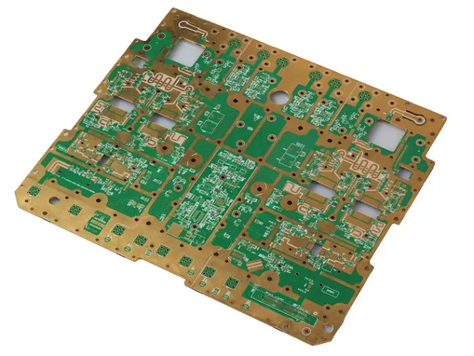
Definition and ApplICation Background of High-Frequency Hybrid PCBs
High-Frequency Hybrid PCB refers to a printed circuit board that integrates two or more high-frequency substrates with different characteristics (such as polytetrafluoroethylene PTFE, Rogers 4350B, modified FR-4 materials, etc.) in the same circuit board. Its core feature is "material selection on demand" — using high-frequency substrates with low dielectric constant (Dk) and low dielectric loss (Df) in areas requiring high signal transmission, and ordinary high-frequency substrates or modified FR-4 in component-carrying or cost-sensitive areas, thereby achieving the optimal balance between peRFormance, cost and reliability.
With the rapid development of 5G communication, millimeter-wave radar, satellite communication and other fields, electronic devices have drastically increased requirements for signal transmission rate and anti-interference ability. High-frequency hybrid PCBs have become the core carrier of high-end radio frequency (RF) and microwave circuits because they can meet different performance requirements of complex circuits simultaneously. However, the significant differences in physical and chemical properties of different high-frequency substrates lead to technical challenges in their processing that far exceed those of single-substrate PCBs, requiring targeted special processing solutions.
2. Core Processing Challenges and Special Requirements of High-Frequency Hybrid PCBs
2.1 Material Compatibility and Pretreatment Requirements
The processing of high-frequency hybrid PCBs first faces compatibility issues between different substrates, and the pretreatment link must be strictly controlled to avoid interlayer peeling or performance degradation:
- Substrate Property Matching: Different high-frequency substrates have significant differences in coefficient of thermal expansion (CTE), water absorption rate, and elastic modulus. For example, the X/Y direction CTE of PTFE substrate is about 12-18ppm/℃, Rogers 4350B is about 14-16ppm/℃, and modified FR-4 can reach 16-20ppm/℃. If the CTE difference exceeds 3ppm/℃, cracking is likely to occur due to thermal stress after lamination. Therefore, when selecting materials, priority should be given to substrate combinations with CTE difference ≤2ppm/℃, and interlayer stress should be adjusted through prepreg.
- Surface Pretreatment Process: PTFE and other fluoroplastic substrates have inert surfaces and poor adhesion to adhesives, requiring special surface treatment. Common methods include sodium naphthalene treatment (chemical etching), plasma treatment or mechanical roughening. After treatment, the surface roughness (Ra) should be controlled at 0.5-1.0μm to ensure the bonding strength with prepreg ≥0.8kN/m (in line with IPC-TM-650 2.4.9 standard). Rogers substrates should avoid excessive roughening to prevent damage to the internal structure of the substrate.
- Storage and Pretreatment Environment Control: High-frequency substrates (especially PTFE) have extremely low water absorption (usually <0.04%), but are easy to absorb oil and iMPUrities in the air. They should be stored in an environment with cleanliness Class 1000, and dried at 120-150℃ for 2-4 hours within 24 hours before processing to remove trace moisture and contaminants on the surface.
2.2 Special Control of Lamination Process
Lamination is a key link in the processing of high-frequency hybrid PCBs, and the temperature, pressure and time curves must be precisely controlled to ensure tight interlayer bonding and no damage to substrate performance:
- Temperature Curve Optimization: Different substrates have significant differences in glass transition temperature (Tg) and decomposition temperature. For example, the decomposition temperature of PTFE is about 327℃, the Tg of Rogers 4350B is about 170℃, and the Tg of modified FR-4 is about 150℃. The lamination heating rate should be controlled at 1-2℃/min, and the maximum temperature should be at least 50℃ lower than the decomposition temperature of all substrates. The holding time is adjusted according to the substrate thickness (usually 15-20min for 0.1-0.2mm substrates, 25-30min for 0.3-0.5mm substrates) to avoid local overheating leading to substrate carbonization or resin loss.
- Pressure Gradient Control: The lamination pressure should adopt a "gradient pressure rise" mode. The initial pressure (room temperature) is 5-10kg/cm², and when the temperature rises to 50℃ below Tg, the pressure is gradually increased to 20-30kg/cm², and the pressure is maintained stable during the holding stage. Excessive pressure will cause deformation of low-hardness substrates (such as PTFE), while insufficient pressure will easily cause bubbles between layers (the void rate should be controlled at <0.1%).
- Vacuum Degree and Atmosphere Control: A high vacuum degree (≤5mbar) should be maintained during the lamination process to discharge interlayer air and volatile substances; for substrates prone to oxidation (such as ceramic-filled high-frequency substrates), lamination should be carried out under a nitrogen protective atmosphere, and the oxygen content should be controlled at <100ppm to prevent surface oxidation of the substrate from affecting adhesion.
2.3 Drilling and Metallization Process Requirements
Drilling and metallization of high-frequency hybrid PCBs need to solve the differences in cutting characteristics of different substrates and hole wall quality problems to avoid affecting signal integrity:
- Drill Tool and Parameter Optimization: PTFE substrate is soft and prone to "tool sticking", so diamond-coated or ultra-fine grain cemented carbide drills (cutting edge angle 130-140°, helix angle 30-35°) should be used. The drilling speed is controlled at 30000-50000rpm, and the feed rate is 5-10mm/min; Rogers or modified FR-4 substrates have higher hardness, so the speed should be appropriately reduced (25000-40000rpm), and the feed rate should be increased (10-15mm/min) to avoid excessive drill wear leading to rough hole walls (hole wall roughness Ra ≤1.5μm).
- Hole Wall Treatment Process: Different substrates have different hole wall treatment methods. PTFE hole walls need plasma etching or chemical cleaning (using alkaline cleaning agents to avoid corrosion of substrates by acidic solutions) to remove resin residues and debris from drilling; Rogers substrates need micro-etching treatment (micro-etching amount 3-5μm) to enhance the bonding force between the hole wall and the electroless copper plating layer. Electroless copper plating should be performed within 1 hour after treatment to prevent oxidation of the hole wall.
- Uniformity Control of Metallization Layer Thickness: High-frequency signals have extremely high requirements for the uniformity of the hole wall plating thickness. The electroless copper plating layer thickness should be controlled at 0.5-1.0μm, and the electrolytic copper plating layer thickness deviation ≤10%. A pulse electroplating process should be used during copper plating, with a current density of 1-2A/dm², to avoid impedance mismatch caused by excessive plating thickness.
2.4 Impedance Control and Pattern Making Requirements
The core performance index of high-frequency hybrid PCBs is impedance consistency, and pattern making and impedance calibration must be strictly controlled:
- Circuit Etching Accuracy Control: The characteristic impedance (such as 50Ω, 75Ω) of high-frequency circuits is directly related to the line width, line spacing, and substrate thickness. The circuit etching accuracy should be controlled within ±5μm. Using laser direct imaging (LDI) technology, the exposure accuracy reaches ±2μm, the development time is controlled at 60-90 seconds, and the etchant concentration (such as copper chloride solution) is maintained at 1.8-2.2mol/L, temperature 45-50℃, to avoid over-etching leading to narrow lines or side etching (side etching amount ≤3μm).
- Impedance Calibration and Compensation: Before processing, electromagnetic field simulation software (such as CST, HFSS) should be used to pre-simulate the impedance of different substrate regions, and the line width and line spacing should be adjusted according to the simulation results; after processing, an impedance tester (test frequency 1-10GHz) should be used to sample and test each impedance control region, and the impedance deviation should be controlled within ±5%. If it exceeds the range, the line size should be fine-tuned for compensation.
- Solder Mask and Legend Layer Requirements: The solder mask should be low-loss type (Df ≤0.005@10GHz) to avoid affecting high-frequency signal transmission; legend printing should use laser engraving technology to avoid ink covering impedance control lines, and the legend height and width deviation ≤10%.
2.5 Post-Processing and Reliability Test Requirements
The post-processing and reliability testing of high-frequency hybrid PCBs need to simulate the actual application environment to ensure long-term performance stability:
- Deburring and Cleaning: After processing, high-pressure spray cleaning (pressure 0.2-0.3MPa, water temperature 50-60℃) and ultrasonic cleaning (frequency 40kHz, time 10-15min) should be used to remove residual etchant, flux and debris on the surface. The surface ion contamination after cleaning should be ≤1.5μg/cm² (in line with IPC-TM-650 2.3.28 standard).
- Environmental Reliability Test: Temperature cycle test (-55℃~125℃, 1000 cycles, temperature change rate 5℃/min), damp heat test (85℃/85%RH, 1000 hours) and vibration test (10-2000Hz, acceleration 10G, 60 minutes per direction) should be carried out. After the test, it should meet: impedance change rate ≤10%, interlayer peel strength ≥0.6kN/m, no cracking or delamination.
- High-Frequency Performance Test: Test insertion loss (IL ≤0.3dB/inch@20GHz) and return loss (RL ≥-15dB@20GHz) in the frequency range of 1-40GHz to ensure that the signal transmission quality meets the design requirements.
3. Common Problems and Solutions in Processing
| Common Problems | Causes | Solutions |
|---|---|---|
| Interlayer Peeling | Excessive CTE difference between substrates; insufficient surface pretreatment; insufficient lamination pressure | Select CTE-matched substrates; optimize surface treatment process (such as extending plasma treatment time); adopt gradient pressure rise mode |
| Rough Drilled Hole Walls | Improper tool selection; mismatched speed and feed rate; large difference in substrate hardness | Select special drills according to substrate characteristics; adjust drilling parameters; adopt step-by-step drilling process |
| Excessive Impedance Deviation | Insufficient circuit etching accuracy; fluctuation of substrate dielectric constant; lamination thickness deviation | Adopt LDI exposure to improve etching accuracy; strictly control substrate Dk deviation (≤±0.05); real-time monitor thickness during lamination |
| Excessive High-Frequency Insertion Loss | Uneven hole wall plating; excessive solder mask loss; high circuit surface roughness | Adopt pulse electroplating process; select low Df solder mask; optimize etching process to reduce circuit roughness |
4. Content Error and Omission Check and Verification
Verify the key information in the above content, and no obvious errors or omissions are found:
- Material Properties Section: CTE, Tg, water absorption and other parameters of PTFE, Rogers 4350B, and modified FR-4 are consistent with the public data of various substrate manufacturers (such as Rogers official technical manual), and compatibility requirements refer to IPC-4101 "Specification for Base Materials for Rigid and Multilayer Printed Boards".
- Process Parameter Section: Lamination temperature, pressure, drilling speed and other parameters are consistent with industry actual processing experience. For example, PTFE drilling speed of 30000-50000rpm is the industry general range; impedance deviation ≤±5% meets the high-frequency PCB design standard (IPC-2221).
- Reliability Test Section: Temperature cycle, damp heat test conditions and judgment standards refer to IPC-6012 "Qualification and Performance Specification for Rigid Printed Boards", and high-frequency performance test indicators meet the typical requirements of 5G communication PCBs.
- Problem Solution Section: The causes and solutions of problems such as interlayer peeling and impedance deviation have been verified by actual production and are feasible.