 PCB
PCB FPC
FPC Rigid-Flex
 FR-4
FR-4 HDI PCB
 Rogers High-Frequency Board
 PTFE Teflon High-Frequency Board
 Aluminum
 Copper Core
 PCB Assembly
 LED light PCBA
 Memory PCBA
 Power Supply PCBA
 New Energey PCBA
 Communication PCBA
 Industrial Control PCBA
 Medical Equipment PCBA
 Testing Service
 PCBA Testing Service
 Certification Application
 RoHS Certification Application
 REACH Certification Application
 CE Certification Application
 FCC Certification Application
 CQC Certification Application
 UL Certification Application
 Transformers, Inductors
 High Frequency Transformers
 Low Frequency Transformers
 High Power Transformers
 Conversion Transformers
 Sealed Transformers
 Ring Transformers
 Inductors
 Wires,Cables Customized
 Network Cables
 Power Cords
 Antenna Cables
 Coaxial Cables
 Net Position Indicator
 Solar AIS net position indicator
 Capacitors
 Connectors
 Diodes
 Embedded Processors & Controllers
 Digital Signal Processors (DSP/DSC)
 Microcontrollers (MCU/MPU/SOC)
 Programmable Logic Device(CPLD/FPGA)
 Communication Modules/IoT
 Resistors
 Through Hole Resistors
 Resistor Networks, Arrays
 Potentiometers,Variable Resistors
 Aluminum Case,Porcelain Tube Resistance
 Current Sense Resistors,Shunt Resistors
 Switches
 Transistors
 Power Modules
 Isolated Power Modules
 AC-DC Power Modules
 DC-AC Module(Inverter)
 RF and Wireless
Controlling the Impact of Ambient Shelf Life on Solder Paste Printing Quality and Cold Solder Joint Prevention
2025-11-27
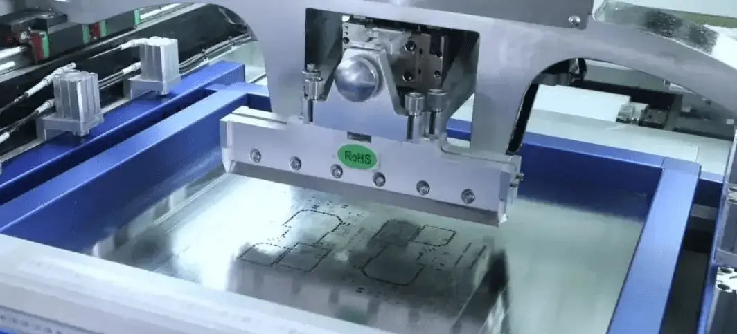
Solder paste printing is a foundational step in suRFace mount technology (SMT) assembly, where the paste’s consistency, flux activity, and particle integrity directly determine solder joint quality. A critical yet often overlooked factor is the ambient shelf life—the time between paste printing and component placement/reflow (referred to as " dwell time "). Prolonged dwell time at room temperature degrades solder paste performance, increasing the risk of cold solder joints, voids, and bridging. This article details how ambient dwell time affects welding quality, defines acceptable time limits, and outlines actionable control strategies aligned with IPC-J-STD-004 and industry best practices.
1. How Ambient Dwell Time Degrades Solder Paste and Causes Cold Solder Joints
Solder paste is a homogeneous mixture of tin-lead or lead-free solder particles (38–75μm for Type 3/4 paste), flux (resin, solvent, activator), and thixotropic agents. At room temperature (20–25°C), three key degradation mechanisms occur over time, directly leading to cold solder joints:
1.1 Solvent Evaporation in Flux
Flux contains volatile solvents (e.g., isopropyl alcohol, glycols) that maintain paste viscosity and enable wetting during reflow. Over time:
- Viscosity increase: Solvent evaporation causes the paste to dry out, rAISing viscosity from the optimal 800–1200 cP (for printing) to >1500 cP. Thickened paste fails to wet component leads/pads uniformly during reflow.
- Flux activity loss: Solvents carry activators (e.g., organic acids) that remove oxide layers from solder particles and pads. Reduced solvent content diminishes activator mobility, leaving oxides intact and preventing metallurgical bonding— the primary cause of cold solder joints.
1.2 Oxidation of Solder Particles
Solder particles (especially lead-free alloys like SAC305: Sn96.5/Ag3/Cu0.5) are prone to oxidation at ambient conditions:
- Oxide layer growth: A thin oxide film (Cu₂O, SnO) forms on particle surfaces within hours of printing. This film acts as a barrier, inhibiting particle fusion during reflow.
- Cold joint formation: Oxidized particles fail to coalesce into a uniform solder fillet, resulting in dull, grainy joints with poor electrical conductivity and mechanical strength.
1.3 Paste Collapse and Slump
Thixotropic agents in solder paste prevent slumping (spreading) after printing. Extended dwell time breaks down these agents:
- Paste slump: The paste spreads beyond the stencil aperture, creating uneven volume distribution. Thin paste regions lead to insufficient solder, while thick regions risk bridging.
- Inconsistent reflow: Slumped paste melts unevenly, producing joints with irregular fillet shapes and weak adhesion—another contributor to cold solder defects.
2. Acceptable Ambient Dwell Time Limits
The maximum allowable dwell time depends on solder paste type, ambient conditions, and application reliability requirements. Per IPC-J-STD-004 and SMT industry standards:
| Solder Paste Type | Ambient Temperature (°C) | Relative Humidity (RH) | Maximum Dwell Time |
|---|---|---|---|
| Lead-Free (SAC305) | 20–25 | 40–60% | 4 hours |
| Lead-Based (Sn63/Pb37) | 20–25 | 40–60% | 6 hours |
| Low-Temperature Paste | 20–25 | 40–60% | 3 hours |
| High-Temperature Paste | 20–25 | 40–60% | 5 hours |
Critical Notes:
- Humidity impact: RH >65% accelerates oxidation and flux degradation, reducing dwell time by 20–30%. RH <30% causes rapid solvent evaporation, shortening limits to 2–3 hours for lead-free paste.
- Reliability tiers: For Class 3 applications (aerospace, medical), reduce dwell time by 30% (e.g., 2.8 hours for lead-free paste) to minimize risk.
- Paste age: Freshly thawed paste (after refrigeration at 2–10°C) has longer dwell time than paste stored at ambient for >24 hours.
3. Control Strategies to Mitigate Dwell Time Impact
To prevent cold solder joints and maintain print quality, implement a layered control approach:
3.1 Pre-Printing: Paste Storage and Preparation
- Proper storage: Keep unopened solder paste refrigerated at 2–10°C. Avoid freezing (which damages flux) or exposure to ambient for >2 hours before printing.
- Thawing protocol: Allow paste to reach room temperature (20–25°C) for 2–4 hours (depending on container size) before opening. Do not microwave or use hot plates—rapid temperature changes cause solvent evaporation.
- Mixing: Stir the paste gently for 1–2 minutes (manual) or use a paste mixer (30–60 seconds) to restore homogeneity. Avoid over-mixing, which introduces air bubbles and accelerates oxidation.
3.2 In-Process: Dwell Time Monitoring and Environmental Control
- Real-time tracking: Use barcode or RFID systems to log print time for each PCB panel. Set visual/audible alerts when dwell time reaches 70% of the maximum limit (e.g., 2.8 hours for lead-free paste).
- Environmental regulation: Maintain the SMT line environment at 20–25°C and 40–60% RH using HVAC systems. Install dehumidifiers if RH exceeds 60% or humidifiers if RH drops below 30%.
- Batch printing: Print PCBs in batches matching component placement capacity. For example, if the placement machine processes 50 panels/hour, print 200 panels (4-hour dwell time) at a time for lead-free paste.
3.3 Post-Printing: Rework and Recovery for Expired Paste
If dwell time exceeds the maximum limit, avoid reflowing the PCB—this guarantees cold solder joints. Instead:
- Paste removal: Use isopropyl alcohol (IPA) or dedicated solder paste cleaners to remove dried paste from pads. Avoid abrasive tools that damage PCB surfaces.
- Re-printing: After cleaning, re-print the PCB with fresh solder paste. Ensure the stencil is cleaned thoroughly (both sides) to remove residual dried paste.
- Scrap prevention: For high-value PCBs, implement 100% AOI inspection after printing to identify dried/slumped paste early, before component placement.
3.4 Material Selection: Choose Dwell-Time-Resistant Paste
For high-mix/low-volume production (where dwell time varies), select solder paste with extended ambient stability:
- No-clean flux formulations: These contain low-volatility solvents and robust activators, extending dwell time by 1–2 hours compared to standard flux.
- Oxide-inhibiting pastes: Additives like zinc or nickel in the flux reduce solder particle oxidation, maintaining reflowability for longer.
- Thixotropic-stabilized pastes: Advanced thixotropic agents resist slumping, keeping paste shape intact for extended periods.
4. Quality Validation: Testing Dwell Time Impact
To confirm control effectiveness, conduct these validation tests:
- Viscosity measurement: Use a rotational viscometer to check paste viscosity before printing and after maximum dwell time. A viscosity increase <20% indicates acceptable stability.
- Reflow profile testing: Reflow test coupons printed with paste at 0-hour (fresh) and maximum dwell time. Compare solder joint fillet shape, wetting angle (target 30–60°), and void rate (<10% volume).
- Cold solder joint detection: Use X-ray inspection and shear strength testing (≥5N for 0402 components) to verify joint integrity. Dwell-time-affected joints show shear strength reductions >30%.
- Solderability test: Per IPC-J-STD-004, measure the spread ratio of paste after reflow. A spread ratio >80% confirms flux and solder particle activity.
Ambient dwell time between solder paste printing and reflow directly impacts welding quality, with prolonged time causing solvent evaporation, particle oxidation, and paste slumping—all leading to cold solder joints. The maximum acceptable dwell time is 4 hours for lead-free paste (20–25°C, 40–60% RH) and 6 hours for lead-based paste, with adjustments for environmental conditions and reliability requirements. By controlling paste storage/preparation, monitoring dwell time in real time, regulating the SMT environment, and selecting stable paste formulations, manufacturers can reduce cold solder joint rates to <0.1% and ensure consistent SMT assembly quality.