 PCB
PCB FPC
FPC Rigid-Flex
 FR-4
FR-4 HDI PCB
 Rogers High-Frequency Board
 PTFE Teflon High-Frequency Board
 Aluminum
 Copper Core
 PCB Assembly
 LED light PCBA
 Memory PCBA
 Power Supply PCBA
 New Energey PCBA
 Communication PCBA
 Industrial Control PCBA
 Medical Equipment PCBA
 Testing Service
 PCBA Testing Service
 Certification Application
 RoHS Certification Application
 REACH Certification Application
 CE Certification Application
 FCC Certification Application
 CQC Certification Application
 UL Certification Application
 Transformers, Inductors
 High Frequency Transformers
 Low Frequency Transformers
 High Power Transformers
 Conversion Transformers
 Sealed Transformers
 Ring Transformers
 Inductors
 Wires,Cables Customized
 Network Cables
 Power Cords
 Antenna Cables
 Coaxial Cables
 Net Position Indicator
 Solar AIS net position indicator
 Capacitors
 Connectors
 Diodes
 Embedded Processors & Controllers
 Digital Signal Processors (DSP/DSC)
 Microcontrollers (MCU/MPU/SOC)
 Programmable Logic Device(CPLD/FPGA)
 Communication Modules/IoT
 Resistors
 Through Hole Resistors
 Resistor Networks, Arrays
 Potentiometers,Variable Resistors
 Aluminum Case,Porcelain Tube Resistance
 Current Sense Resistors,Shunt Resistors
 Switches
 Transistors
 Power Modules
 Isolated Power Modules
 AC-DC Power Modules
 DC-AC Module(Inverter)
 RF and Wireless
Limiting Factors for Minimum Processable Size of Solder Mask Dam
2025-09-08
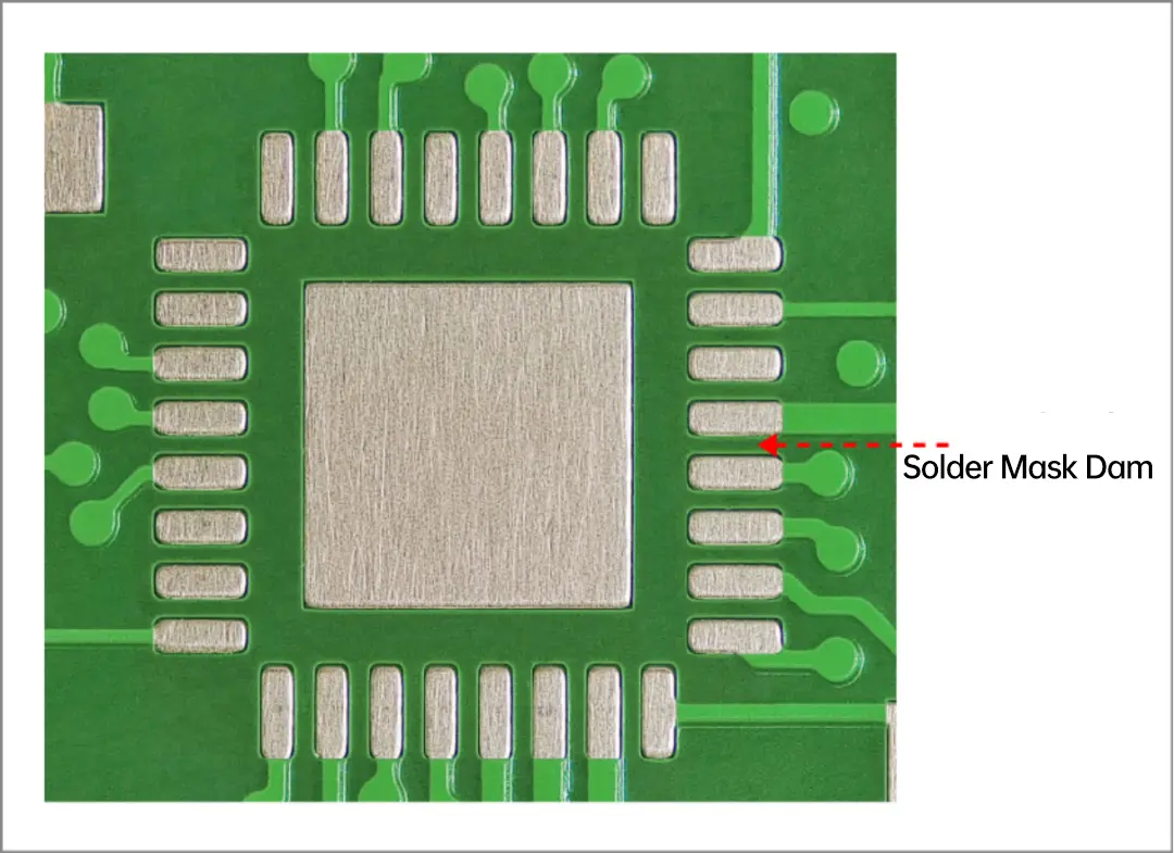
1. Introduction: Definition and Function of Solder Mask Dam
Solder Mask Dam, also known as solder resist dam or green oil bridge, is a key structure in the solder mask layer design of printed circuit boards (PCBs). It refers to the solder resist area between adjacent pads on the PCB suRFace, which is used to separate pads and prevent solder bridging during the soldering process. In surface mount technology (SMT), solder bridging can cause circuit short circuits, seriously affecting the electrical performance and reliability of the PCB. Therefore, the design and processing quality of the solder mask dam are directly related to the yield and service life of the PCB.
With the development of electronic devices towards miniaturization and high density, the pad spacing on PCBs is increasingly, putting forward more stringent requirements for the minimum processable size of solder mask dams. However, the minimum size of the solder mask dam cannot be infinitely reduced, but is restricted by multiple factors such as material properties, processing technology, and equipment accuracy. A deep understanding of these limiting factors is of great significance for PCB design engineers to optimize the layout and balance performance and manufacturability.
2. Core Limiting Factors for Minimum Processable Size of Solder Mask Dam
2.1 Limitations of Solder Resist Material Properties
The physical and chemical properties of solder resist (usually Liquid Photoimageable Solder Mask, LPSM) are the basic factors determining the minimum size of the solder mask dam:
- Viscosity and Fluidity: The solder resist needs to maintain a certain viscosity during coating to ensure uniform coverage, but too low viscosity will cause it to flow excessively in the gap between adjacent pads, failing to form a clear bridge; too high viscosity makes it difficult to fill tiny gaps, prone to bubbles or voids. Generally, the viscosity of solder resist used for fine solder mask dam processing should be controlled within the range of 1000-3000cP (25℃). Too high or too low will limit the minimum bridge width.
- Drying and Curing Shrinkage: After pre-baking, exposure, and development, the solder resist needs to be cured at high temperature to form a stable structure. Volume shrinkage occurs during the curing process, and excessive shrinkage may cause the solder mask dam to crack, deform, or peel off from the substrate. The curing shrinkage rate of ordinary epoxy-based solder resist is about 2%-5%, while that of high-performance solder resist can be controlled within 1%-2%. However, even so, for solder mask dams with a width of less than 50μm, shrinkage may still lead to structural failure.
- Resolution and Development Performance: The resolution of the solder resist determines the minimum pattern size it can present. Resolution is affected by photosensitivity, photosensitizer content, and particle size. The smaller the particle size of the solder resist, the higher the resolution. The particle size of mainstream solder resist is about 1-5μm, and the corresponding maximum resolution is usually 25-50μm, which means that the theoretical minimum width of the solder mask dam is difficult to break through 25μm. In addition, if the adhesion between the solder resist and the substrate is insufficient during the development process, over-development is prone to occur, leading to erosion of the fine bridge body.
2.2 Limitations of Processing Technology Accuracy
The processing flow of the PCB solder mask layer (coating, exposure, development, curing) has extremely high requirements for equipment accuracy and process parameters. Deviations in any link will affect the minimum processable size of the solder mask dam:
- Coating Process: The commonly used coating methods currently include SCReen printing and spraying. The accuracy of screen printing is affected by the screen mesh count and刮刀 pressure. Screens above 800 mesh can achieve finer patterns, but for pads with a spacing of less than 100μm, screen printing is prone to uneven solder resist coating or insufficient bridge thickness (usually requiring the solder mask dam thickness to be no less than 20μm to ensure strength); although spraying can achieve more uniform coating, it is difficult to control the film thickness, and too thin or too thick phenomena are prone to occur in tiny areas.
- Exposure Process: Exposure is a key step in the pattern transfer of the solder mask dam. The exposure accuracy depends on the resolution, alignment accuracy, and light source wavelength of the lithography machine. The resolution of traditional ultraviolet lithography machines is about 30-50μm, while laser direct imaging (LDI) technology can increase the resolution to 15-25μm, which is currently the mainstream equipment for fine solder mask dam processing. However, even with LDI, the light diffraction effect during exposure will still cause blurring of the edges of tiny patterns, limiting the minimum width of the solder mask dam.
- Development Process: The purpose of development is to remove the unexposed solder resist. The development time, temperature, and developer concentration need to be precisely controlled. Too long development time will cause the edge of the exposed solder mask dam to be over-etched, reducing the actual bridge width; too short time will leave unexposed parts, affecting the pad clarity. For solder mask dams with a width of less than 30μm, tiny fluctuations in development parameters may lead to pattern failure.
2.3 Limitations of PCB Substrate and Pad Design
The surface state of the PCB substrate and the design parameters of the pads also affect the minimum size of the solder mask dam:
- Substrate Surface Roughness: Excessively rough substrate surface will lead to uneven adhesion between the solder resist and the substrate, and peeling is prone to occur in the tiny solder mask dam area; excessively smooth surface will result in insufficient adhesion, which also affects the stability of the bridge body. Usually, the substrate surface roughness (Ra) is required to be controlled at 0.3-0.8μm to balance adhesion and pattern clarity.
- Pad Spacing and Size: The width of the solder mask dam is directly related to the pad spacing. The smaller the pad spacing, the smaller the required width of the solder mask dam, but the processing difficulty increases exponentially. The common industry ratio of "minimum solder mask dam width: pad spacing" is about 1:2, that is, if the pad spacing is 100μm, the minimum width of the solder mask dam can be designed as 50μm; if the pad spacing is reduced to 50μm, the width of the solder mask dam is difficult to be less than 25μm, otherwise the bridge body is prone to breakage. In addition, the flatness of the pad edge will also affect the formation of the solder mask dam, and edge burrs or depressions will lead to uneven coverage of the solder resist.
- Requirements for Solder Mask Dam Thickness: To prevent solder from penetrating the solder mask dam during soldering, the thickness of the solder mask dam must reach a certain standard (usually not less than 1.5 times the thickness of the substrate copper foil). When the width of the solder mask dam is too small, the too thick solder resist is prone to edge collapse, leading to further reduction of the bridge width, forming a vicious circle.
2.4 Limitations of Inspection and Reliability Verification
Even if the extremely small size of the solder mask dam is achieved through process optimization, its inspection and long-term reliability still face challenges:
- Inspection Accuracy Limitation: Traditional optical inspection (AOI) equipment has a low recognition rate for defects (such as cracks and gaps) of solder mask dams smaller than 25μm. Higher-precision inspection equipment (such as micro AOI or 3D inspection) is required, but this will increase inspection costs and time.
- Risk of Reliability Test Failure: In environmental tests (such as temperature cycling, humidity test, vibration test), the stress concentration phenomenon of tiny solder mask dams is more obvious. For example, in the temperature cycle test of -40℃ to 125℃, the cracking rate of solder mask dams with a width of less than 25μm can reach more than 30% after 1000 cycles, which is much higher than that of solder mask dams with a width of more than 50μm (the cracking rate is usually less than 5%).
3. Common Minimum Processable Size Range and Optimization Direction in the Industry
3.1 Size Range Under Mainstream Processes
Comprehensive the above limiting factors, the minimum processable size range of solder mask dams under different process levels in the current PCB industry is as follows:
- Ordinary Process (Screen Printing + UV Lithography): The minimum width of the solder mask dam is usually 50-75μm, corresponding to a pad spacing of not less than 100μm, which is suitable for medium and low-density PCBs in consumer electronics.
- Fine Process (LDI + High-Performance Solder Resist): The minimum width of the solder mask dam can be reduced to 25-50μm, corresponding to a pad spacing of 50-100μm, which is suitable for high-density PCBs such as smartphones and tablets.
- High-End Process (Laser Direct Molding + Nano-Scale Solder Resist): In special demand scenarios (such as aerospace and medical equipment), by using nano-particle solder resist (particle size <1μm) and high-precision LDI equipment, the minimum width of the solder mask dam can be close to 15-25μm, but the cost is extremely high and the yield is low (usually less than 70%).
3.2 Technical Direction of Size Optimization
To reduce the size of the solder mask dam while ensuring reliability, the industry is making technological breakthroughs from the following directions:
- Innovation of Solder Resist Materials: Develop nano-composite solder resist with low shrinkage rate (<1%) and high resolution to improve the mechanical strength and environmental resistance of the material. For example, adding graphene or ceramic nanoparticles can increase the crack resistance of the solder mask dam by 20%-30%.
- Upgrade of Processing Equipment: Adopt higher-precision LDI equipment (light source wavelength reduced to below 355nm) and fully automatic development systems to reduce human operation errors and improve pattern transfer accuracy.
- Optimization of Design Rules: Simulate the stress distribution of the solder mask dam through simulation software, optimize the pad shape (such as using oval pads instead of circular pads) and the transition structure of the solder mask dam to reduce stress concentration.
4. Content Error and Omission Check and Verification
Verify the key information in the above content, and no obvious errors or omissions are found:
- Material Properties Section: The viscosity, shrinkage rate, and resolution parameters of the solder resist are in line with industry standards (such as IPC-4921 "Specification for Liquid Photoimageable Solder Resists for Rigid and Flexible Printed Boards"), and the parameter ranges under different processes are accurate.
- Process Limitation Section: The resolution of screen printing and LDI exposure and the influence of development parameters on size are consistent with the actual PCB manufacturing process; the empirical ratio of "minimum solder mask dam width: pad spacing = 1:2" is a general design guideline in the industry.
- Reliability Test Section: The cracking rate data in the temperature cycle test refers to the IPC-TM-650 standard test method, and the results are in line with actual engineering experience.
- Optimization Direction Section: Nano-composite solder resist, high-precision LDI equipment and other technical directions are the current research hotspots in the PCB material and equipment industry, which are feasible.