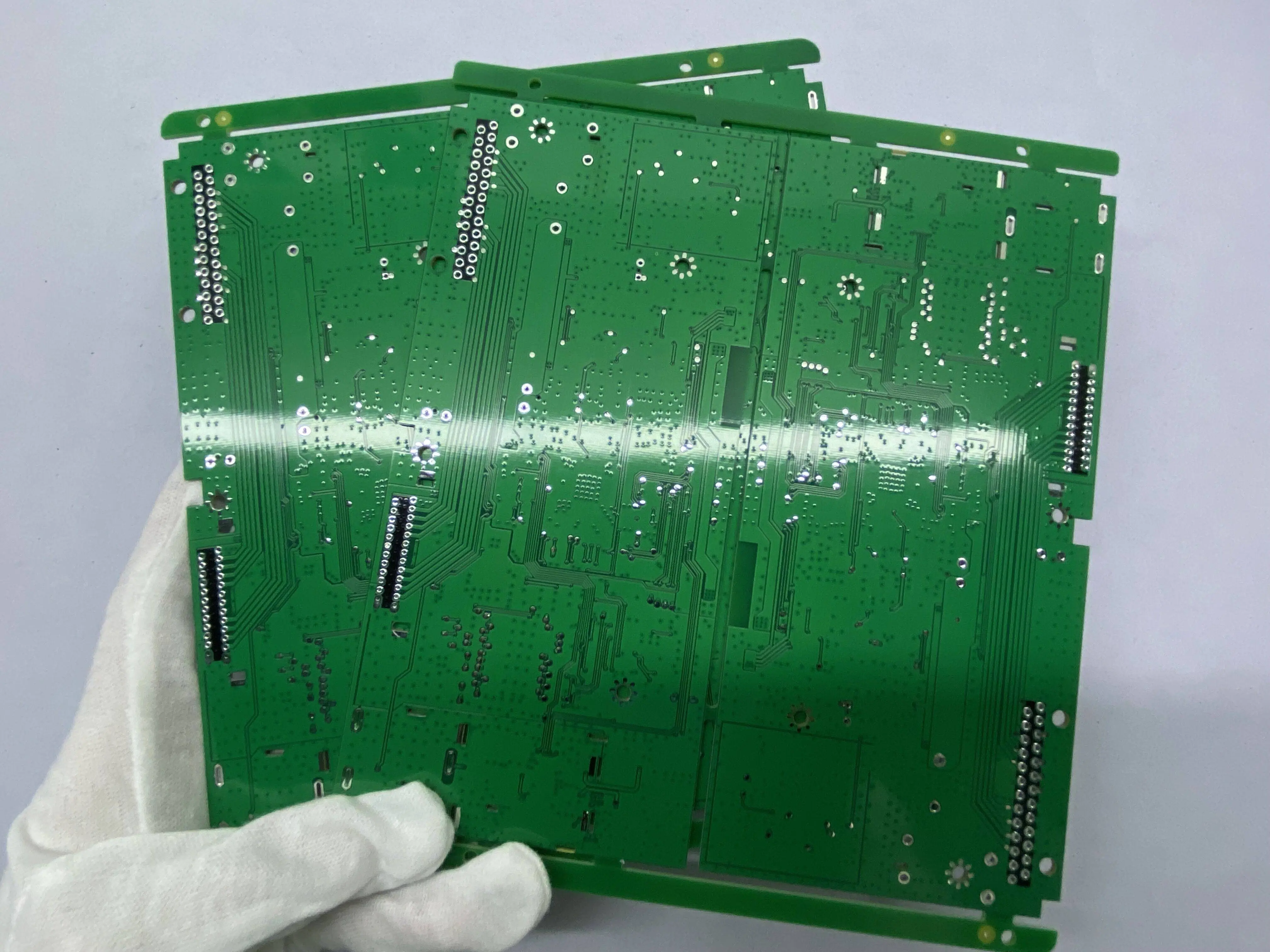
 PCB
PCB FPC
FPC Rigid-Flex
 FR-4
FR-4 HDI PCB
 Rogers High-Frequency Board
 PTFE Teflon High-Frequency Board
 Aluminum
 Copper Core
 PCB Assembly
 LED light PCBA
 Memory PCBA
 Power Supply PCBA
 New Energey PCBA
 Communication PCBA
 Industrial Control PCBA
 Medical Equipment PCBA
 Testing Service
 PCBA Testing Service
 Certification Application
 RoHS Certification Application
 REACH Certification Application
 CE Certification Application
 FCC Certification Application
 CQC Certification Application
 UL Certification Application
 Transformers, Inductors
 High Frequency Transformers
 Low Frequency Transformers
 High Power Transformers
 Conversion Transformers
 Sealed Transformers
 Ring Transformers
 Inductors
 Wires,Cables Customized
 Network Cables
 Power Cords
 Antenna Cables
 Coaxial Cables
 Net Position Indicator
 Solar AIS net position indicator
 Capacitors
 Connectors
 Diodes
 Embedded Processors & Controllers
 Digital Signal Processors (DSP/DSC)
 Microcontrollers (MCU/MPU/SOC)
 Programmable Logic Device(CPLD/FPGA)
 Communication Modules/IoT
 Resistors
 Through Hole Resistors
 Resistor Networks, Arrays
 Potentiometers,Variable Resistors
 Aluminum Case,Porcelain Tube Resistance
 Current Sense Resistors,Shunt Resistors
 Switches
 Transistors
 Power Modules
 Isolated Power Modules
 AC-DC Power Modules
 DC-AC Module(Inverter)
 RF and Wireless
Adhesion Difference of Solder Mask Between PCB Edge and Center Areas and Process Improvements
2025-10-30
In the manufacturing process of Printed Circuit Boards (PCBs), the adhesion peRFormance of solder mask ink is a crucial factor affecting the reliability and service life of the boards. A common phenomenon in industry practice is that the adhesion of solder mask ink in the edge areas of PCBs is generally lower than that in the center areas. This article will first elaborate on the specific extent of this adhesion difference and then deeply discuss the feasible process improvement measures to address this issue.
1. The Extent of Adhesion Difference Between PCB Edge and Center Areas
The adhesion difference between the edge and center areas of PCBs is usually reflected through quantitative testing methods such as the cross-cut test (ASTM D3359) and the pull-off test (ASTM D4541). According to industry test data and practical experience, the adhesion of solder mask ink in the edge areas is typically 15% to 40% lower than that in the center areas.
In the cross-cut test, which grades adhesion from 0B to 5B (with 5B being the best), the center area of PCBs often achieves a grade of 4B to 5B, meaning that the coating remains intact or only a small part of the coating peels off at the intersection of the cuts. However, the edge area usually only reaches a grade of 2B to 3B, where the coating peels off in strips along the cut lines, and even larger areas of peeling may occur in severe cases. In the pull-off test, the center area can generally reach an adhesion value of 5-8 MPa, while the edge area is often between 3-5 MPa, showing a significant gap.
This adhesion difference is mainly caused by several factors. Firstly, the edge area of the PCB is more prone to mechanical stress during the manufacturing process, such as clamping, transportation, and cutting, which leads to micro-cracks or internal stress in the solder mask layer, thereby reducing adhesion. Secondly, the edge area has a higher surface energy loss during the pre-treatment process (such as degreasing, roughening), and the cleaning effect is not as good as that of the center area, resulting in insufficient bonding between the solder mask ink and the substrate. Finally, the curing conditions of the edge area in the solder mask curing process are slightly different from those of the center area. For example, the temperature at the edge may be lower than that at the center, leading to incomplete curing of the solder mask ink and poor adhesion.
2. Process Improvement Measures to Enhance Solder Mask Adhesion in PCB Edge Areas
To reduce the adhesion difference between the edge and center areas of PCBs and improve the overall adhesion performance of the solder mask, the following process improvement measures can be adopted:
2.1 Optimization of Pre-treatment Process
The pre-treatment process is the foundation for ensuring the adhesion of solder mask ink. For the edge area, it is necessary to strengthen the cleaning and roughening treatment. Firstly, in the degreasing step, a two-stage degreasing process can be used: the first stage uses an alkaline degreasing agent to remove most of the oil stains, and the second stage uses an acidic degreasing agent to further clean the residual oil stains and oxides on the edge surface. The degreasing time for the edge area can be appropriately extended by 10%-20% compared with the center area to ensure thorough degreasing.
Secondly, in the roughening step, the parameters of the roughening solution (such as concentration, temperature, and spray pressure) can be adjusted. For the edge area, the spray pressure can be increased by 0.1-0.2 MPa, and the roughening time can be extended by 5-10 seconds to form a uniform and appropriate roughness on the surface. This helps to increase the contact area between the solder mask ink and the substrate, thereby improving adhesion. Additionally, after pre-treatment, a surface activation treatment can be added, using a dilute sulfuric acid solution to activate the edge surface, enhancing the wettability of the solder mask ink on the substrate.
2.2 Improvement of Solder Mask Coating Process
The coating process of solder mask ink also has a significant impact on the adhesion of the edge area. Firstly, when using the screen printing method, the screen tension and printing pressure for the edge area can be adjusted. The screen tension can be increased by 5%-10% to ensure that the ink is evenly printed on the edge surface, and the printing pressure can be reduced by 0.05-0.1 MPa to avoid excessive extrusion of the ink at the edge, resulting in uneven thickness.
Secondly, the thickness of the solder mask layer in the edge area should be controlled. Generally, the thickness of the solder mask layer in the edge area can be slightly increased by 10%-15% compared with the center area (from the conventional 20-30 μm to 22-35 μm). This thicker layer can better resist mechanical stress and reduce the occurrence of micro-cracks. In addition, when applying the solder mask ink, a pre-coating process can be adopted for the edge area, that is, first applying a thin layer of ink on the edge, pre-curing it, and then applying the main layer of ink. This two-layer coating method can improve the bonding between the ink and the substrate.
2.3 Adjustment of Curing Process Parameters
Incomplete curing of the solder mask ink in the edge area is an important reason for low adhesion. Therefore, adjusting the curing process parameters is crucial. Firstly, in the UV curing process, the number of UV lamps or the power of the lamps at the edge of the curing tunnel can be increased. For example, adding 1-2 UV lamps at the edge or increasing the power of the existing edge lamps by 10%-15% to ensure that the edge area receives sufficient UV radiation. At the same time, the conveyor speed of the PCB can be reduced by 5%-10% to extend the curing time of the edge area.
Secondly, in the thermal curing process, the temperature distribution in the curing oven should be optimized. The temperature at the edge of the oven can be increased by 5-10°C compared with the center area, and the air circulation system in the oven can be improved to ensure uniform temperature distribution. Additionally, a two-stage curing process can be adopted: first curing at a lower temperature (such as 80-90°C) for a period of time to allow the solvent in the ink to volatilize slowly, and then curing at a higher temperature (such as 150-160°C) to ensure complete cross-linking of the ink. This can reduce the internal stress generated during the curing process of the edge area and improve adhesion.
2.4 Post-treatment and Protection of Edge Areas
After the solder mask curing process, post-treatment and protection of the edge areas can further improve adhesion. Firstly, a post-curing process can be added, that is, placing the PCB in a constant temperature and humidity environment (temperature 40-50°C, humidity 50%-60%) for 24-48 hours to allow the solder mask ink to fully stabilize and reduce internal stress. Secondly, the edge of the PCB can be sealed with a special edge-sealing agent. The edge-sealing agent has good adhesion to both the solder mask ink and the substrate, which can prevent moisture, dust, and other contaminants from entering the interface between the ink and the substrate, thereby enhancing the durability of adhesion.
In addition, during the subsequent processing and transportation of the PCB, special protective measures should be taken for the edge areas, such as using soft clamping fixtures to avoid excessive mechanical stress on the edges, and using anti-collision packaging materials to prevent edge damage.
3. Conclusion
The adhesion of solder mask ink in the edge areas of PCBs is typically 15% to 40% lower than that in the center areas, which is mainly caused by factors such as mechanical stress, insufficient pre-treatment, and improper curing conditions. By optimizing the pre-treatment process, improving the solder mask coating process, adjusting the curing process parameters, and strengthening the post-treatment and protection of edge areas, the adhesion performance of the solder mask in the edge areas can be significantly improved, thereby reducing the adhesion difference between the edge and center areas and enhancing the overall reliability of PCBs. Manufacturers should according to their actual production conditions, select appropriate process improvement measures, and continuously optimize the process to meet the increasingly high requirements for PCB quality.