 PCB
PCB FPC
FPC Rigid-Flex
 FR-4
FR-4 HDI PCB
 Rogers High-Frequency Board
 PTFE Teflon High-Frequency Board
 Aluminum
 Copper Core
 PCB Assembly
 LED light PCBA
 Memory PCBA
 Power Supply PCBA
 New Energey PCBA
 Communication PCBA
 Industrial Control PCBA
 Medical Equipment PCBA
 Testing Service
 PCBA Testing Service
 Certification Application
 RoHS Certification Application
 REACH Certification Application
 CE Certification Application
 FCC Certification Application
 CQC Certification Application
 UL Certification Application
 Transformers, Inductors
 High Frequency Transformers
 Low Frequency Transformers
 High Power Transformers
 Conversion Transformers
 Sealed Transformers
 Ring Transformers
 Inductors
 Wires,Cables Customized
 Network Cables
 Power Cords
 Antenna Cables
 Coaxial Cables
 Net Position Indicator
 Solar AIS net position indicator
 Capacitors
 Connectors
 Diodes
 Embedded Processors & Controllers
 Digital Signal Processors (DSP/DSC)
 Microcontrollers (MCU/MPU/SOC)
 Programmable Logic Device(CPLD/FPGA)
 Communication Modules/IoT
 Resistors
 Through Hole Resistors
 Resistor Networks, Arrays
 Potentiometers,Variable Resistors
 Aluminum Case,Porcelain Tube Resistance
 Current Sense Resistors,Shunt Resistors
 Switches
 Transistors
 Power Modules
 Isolated Power Modules
 AC-DC Power Modules
 DC-AC Module(Inverter)
 RF and Wireless
Detailed Inspection Specifications for SMT Printed Circuit Board (PCB) Pads and Solder Mask
Detailed Inspection Specifications for SMT Printed Circuit Board (PCB) Pads and Solder Mask
In the field of SMT (SuRFace Mount Technology), the printed circuit board (PCB) serves as a core component, and its quality is crucial to the overall assembly process. Therefore, the incoming inspection of PCB boards cannot be ignored. This article will delve into the inspection specifications for PCB pads and solder mask to ensure that the quality of PCB boards meets the requirements of SMT assembly.
I. PCB Pad Inspection Specifications
Pad and Pattern Tolerances
* For SMT Pads (including pads with optical points), the tolerance is ±2mil when the wide side or diameter is greater than 14mil, and ±1mil when it is less than or equal to 14mil. SMD Pads (Solder mask Defined PADs) follow the same rules.
* The size tolerance for BGA Pads should refer to the design specifications, and the measurement position is at the top of the Pad.
* The circular part of the Fiducial mark pattern is φ50±2mil, and the square part is 50±2mil.
Pad Defect Limitations
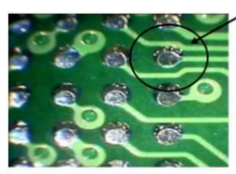
* Defects such as notches, depressions, and pinholes on the pads should not exceed 15% of the soldering area.
* BGA pads must not have defects such as notches, depressions, contaminants, green paint covering the pads, non-wetting, and de-wetting (unless special requirements are stated in the manufacturing requirements).
Solder Surface Requirements
* The solder surface should be flat and free from flattening, exposed copper, or contaminants.
* If the surface treatment is OSP, the pads must not have oxidation, surface blackening, roller marks, uneven film thickness, or bottom copper oxidation discoloration.
* If the surface treatment is chemical gold/silver, there must be no scratches exposing the copper layer and substrate, nor can there be exposed nickel plating or discoloration of the chemical gold/silver surface.
Ring or SMD Pad Requirements
* All rings or SMD pads must not have non-wetting and de-wetting phenomena (de-wetting areas within 5% are acceptable).
* The thickness of the metal surface treatment must meet the specified requirements, such as tin spray within the range of 100μ” to 1000μ” with a tin/lead ratio of Sn63/Pb37; chemical gold thickness should be within 2 to 5μ”, and nickel plating should be applied first, with a nickel thickness of over 100μ”.
Washer Requirements
* The acceptable deviation standard for the drilling and pad offset of the Annular Ring should ensure that the connection area of the conductor or wiring has at least 2mil.
* The Annular Ring for component holes must have at least 2mil. If it is a via hole (Via Hole) not connected to the conductor, it is allowed for the hole to be tangent to the pad, but not to damage it.

SMT Optical Point Requirements
* The optical points must be intact and free from deformation, notches, and depressions.
* They must not have exposed copper, uneven tin surfaces, or tin surface oxidation discoloration.
* They must not have foreign objects, ink, and must not fall off or warp.
PAD Position Tolerance
Before SMD placement and after the Reflow process, the relative position tolerance between the centers of any two pads on the PCB board is ±3mil.
II. Solder Mask (Solder Masker) Inspection Specifications
Flame Resistance and Heat Resistance
* The solder mask must meet the flame resistance requirements of 94V-0 and the heat resistance requirements for soldering.
Circuit Coverage Requirements
The circuits must be fully covered with solder mask, and there must be no tin adherence, copper exposure, or circuit exposure due to missing printing, skipped printing, or other factors (unless specified otherwise in the original design).
Appearance Requirements
* The solder mask surface should have a uniform color, and the surface must be free from impurities, uneven coating, ink accumulation, fingerprints, or other foreign objects that affect appearance.
* The solder mask surface must not have bubbles, peeling, wrinkles, or other phenomena that affect appearance or soldering resistance. The diameter of a single bubble should not exceed 3mm, and its location should not exceed 50% of the spacing between two conductors; no more than 3 bubbles on one side and no more than 5 on both sides.
Pad and Solder Mask Relationship
Pads (including BGA pads) must not have poor development or green paint covering the pads (i.e., scum and solder masker on pad) due to misprinting or exposure, as well as copper exposure on adjacent wires. Green paint must not remain in the holes (except for plugged holes).
Plugged Hole Requirements
All plugged holes must be smooth and free from protrusions. The Annular Ring must not expose copper, and the plugged hole area must not transmit light. The depth of the plugged hole must meet the design requirements. Tin beads or tin plugging are not allowed on tin-plated boards.
Solder Mask Circuit Requirements
For SMD Pad edge-to-edge distances ≥7 mil where ink is required, the solder mask circuit part must not have broken lines (the Solder Dam must not collapse or break).
Adhesion Requirements
* The bare board must not have S/M peeling after metal surface treatment and assembly processes.
* Peeling of the solder mask can be repaired, ensuring flatness and uniformity in color, without affecting telecommunications characteristics, impedance values, or aesthetics.
* The adhesion test should be conducted using 3M SCOTCH NO.600 wide adhesive tape. After adhering and pulling vertically, there should be no peeling.
Thickness and Scratch Requirements
* The thickness of the solder mask on the copper surface (in densely populated areas) is 0.3mil to 0.7mil, and there must be no copper exposure or tin ball adherence at the edges. The total thickness of the solder mask and text on the circuit should not exceed 1.4mil.
* The solder mask must not have scratches exposing copper or the substrate. There should be no more than 3 scratches per side that do not expose copper, each not exceeding 1cm in length, and the scratched areas must not have tin balls or peeling after the solder mask adhesion test.
Solubility Test
Dip isopropanol or trichloroethane onto the board and wipe with a cotton swab for 2 minutes. Visually inspect for discoloration, which is considered a major defect.
Alignment and Hole Requirements
* When aligning the solder mask with the outer layer, it is not allowed for the solder mask to cover the pads.
* When aligning the solder mask with the outer layer SMD Pad, it is allowed for the solder mask to be flush with the pad edge.
* Test holes, via holes (except plugged holes), and component holes must have an Annular Ring with at least 0.002" of tin (gold) washer, and the washer not covered by the solder mask must maintain over 70% tin (gold) wetting area.
* For vias with a diameter of less than 0.4mm that require plugging, they must follow the principle of no copper exposure on both sides of the Annular Ring and no light transmission through the hole.