 PCB
PCB FPC
FPC Rigid-Flex
 FR-4
FR-4 HDI PCB
 Rogers High-Frequency Board
 PTFE Teflon High-Frequency Board
 Aluminum
 Copper Core
 PCB Assembly
 LED light PCBA
 Memory PCBA
 Power Supply PCBA
 New Energey PCBA
 Communication PCBA
 Industrial Control PCBA
 Medical Equipment PCBA
 Testing Service
 PCBA Testing Service
 Certification Application
 RoHS Certification Application
 REACH Certification Application
 CE Certification Application
 FCC Certification Application
 CQC Certification Application
 UL Certification Application
 Transformers, Inductors
 High Frequency Transformers
 Low Frequency Transformers
 High Power Transformers
 Conversion Transformers
 Sealed Transformers
 Ring Transformers
 Inductors
 Wires,Cables Customized
 Network Cables
 Power Cords
 Antenna Cables
 Coaxial Cables
 Net Position Indicator
 Solar AIS net position indicator
 Capacitors
 Connectors
 Diodes
 Embedded Processors & Controllers
 Digital Signal Processors (DSP/DSC)
 Microcontrollers (MCU/MPU/SOC)
 Programmable Logic Device(CPLD/FPGA)
 Communication Modules/IoT
 Resistors
 Through Hole Resistors
 Resistor Networks, Arrays
 Potentiometers,Variable Resistors
 Aluminum Case,Porcelain Tube Resistance
 Current Sense Resistors,Shunt Resistors
 Switches
 Transistors
 Power Modules
 Isolated Power Modules
 AC-DC Power Modules
 DC-AC Module(Inverter)
 RF and Wireless
Specific Placement Defects Caused by Inaccurate Vision System Calibration in SMT Mounters
2025-12-25
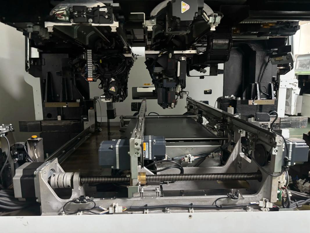
SuRFace Mount Technology (SMT) has become the backbone of modern electronic manufacturing, enabling the precise assembly of miniaturized components (e.g., 01005 chips, micro BGAs, QFNs) onto printed circuit boards (PCBs). The vision system of an SMT mounter is its "eyes," responsible for detecting component positions, PCB pad locations, and aligning the two with micrometer-level accuracy. Calibration of this vision system—including camera calibration, lighting calibration, offset calibration, and scale calibration—is critical to ensuring placement precision. Inaccurate calibration disrupts the vision system’s ability to capture and interpret spatial data, leading to a range of placement defects that compromise PCBA quality, reduce production yields, and increase rework costs.
This article provides a comprehensive analysis of the specific placement defects caused by inaccurate vision system calibration in SMT mounters. It first outlines the core calibration requirements of SMT vision systems, then details each defect’s cause, manifestation, impact, and correlation with calibration errors. References to industry standards such as IPC-A-610 (Acceptability of Electronic Assemblies) and IPC-7351 (Land Pattern Design Standard) are integrated to contextualize defect severity. Practical case studies and mitigation strategies are also included to enhance the article’s applicability for manufacturing engineers and quality control personnel.
1. Core Calibration Requirements of SMT Mounter Vision Systems
The vision system of an SMT mounter typically consists of component cameras (for recognizing component leads/balls), PCB cameras (for identifying PCB fiducials and pads), LED lighting Modules (for enhancing contrast), and image processing software (for analyzing spatial data). Calibration ensures that the vision system’s measurements align with physical reality, with key calibration items including:
1.1 Camera Calibration
Camera calibration corrects optical distortions (radial, tangential) caused by lens imperfections and ensures pixel-to-millimeter conversion accuracy. It involves calibrating the camera’s intrinsic parameters (focal length, principal point) and extrinsic parameters (position relative to the mounter’s motion axes). Inaccurate camera calibration leads to distorted image interpretation and incorrect distance calculations.
1.2 Fiducial Calibration
Fiducials are reference marks on PCBs that guide the vision system to locate the PCB’s exact position. Fiducial calibration involves teaching the vision system to recognize fiducial shapes (circular, square) and calculate the PCB’s offset, rotation, and scaling relative to the mounter’s coordinate system. Poor fiducial calibration results in misalignment between the PCB and the mounter’s motion axes.
1.3 Component Offset Calibration
Component offset calibration accounts for positional deviations between the component’s center (as detected by the vision system) and the mounter’s nozzle center. It includes X/Y offset (lateral deviation), θ offset (rotational deviation), and Z offset (height deviation). Inaccurate offset calibration causes components to be placed off-center or rotated relative to PCB pads.
1.4 Lighting Calibration
Lighting calibration adjusts the intensity, angle, and spectrum of LED lights to optimize contrast between components/PCBs and their backgrounds. Proper lighting ensures clear imaging of component leads, BGA balls, and PCB pads. Poor lighting calibration results in blurred images or misdetection of critical features.
1.5 Scale Calibration
Scale calibration ensures that the vision system’s pixel measurements are converted to accurate physical dimensions (e.g., 1 pixel = 0.01 mm). It is critical for small components (e.g., 01005, 0201) where even 0.1 mm deviations can cause defects.
When any of these calibration items are inaccurate, the vision system transmits erroneous spatial data to the mounter’s motion control system, leading to placement defects. Below is a detailed breakdown of the most common defects and their calibration-related causes.
2. Specific Placement Defects Caused by Inaccurate Calibration
2.1 X/Y Offset Defect (Lateral Misplacement)
X/Y offset defect refers to components being placed laterally off-center relative to their target pads, with deviations exceeding the acceptable limit (typically ±0.1 mm for 0402 components, ±0.2 mm for QFPs). This is the most common defect caused by inaccurate vision system calibration.
2.1.1 Causes (Calibration-Related)
- Inaccurate Camera Extrinsic Calibration: If the camera’s position relative to the mounter’s X/Y axes is not calibrated correctly, the vision system miscalculates the component’s or PCB’s X/Y coordinates. For example, a 0.1 mm error in camera position calibration will directly translate to a 0.1 mm X/Y offset in placement.
- Fiducial Calibration Errors: Failure to accurately calibrate fiducial recognition leads to incorrect PCB positioning. If the vision system misidentifies the fiducial’s center by 0.15 mm, all components on the PCB will be offset by the same amount.
- Scale Calibration Errors: Incorrect pixel-to-physical dimension conversion (e.g., 1 pixel incorrectly calibrated as 0.011 mm instead of 0.01 mm) causes cumulative X/Y deviations, especially for large PCBs or components with wide pad spans.
- Component Offset Calibration Neglect: Failure to calibrate the X/Y offset between the nozzle and the component’s center (e.g., due to nozzle wear or component size changes) leads to lateral misplacement.
2.1.2 Manifestations
Components are shifted left/right, forward/backward relative to their pads. For example: A 0402 resistor is placed such that 30% of its body is off the pad, with one terminal only partially overlapping the pad.A QFP’s leads are misaligned with the PCB’s solder pads, with some leads hanging over the pad edges and others not reaching the pads.A BGA’s solder balls are offset from the PCB’s solder lands, resulting in uneven ball-to-land contact.
2.1.3 Impacts
X/Y offset defects reduce solder joint strength and electrical conductivity. Severe offsets (deviations >50% of component terminal width) cause open circuits or intermittent connections. For BGAs and QFNs, offset can lead to solder bridging between adjacent pads or poor wetting, increasing the risk of thermal fatigue failure during operation. According to IPC-A-610 Class 3 standards (for high-reliability applications), X/Y offsets exceeding 25% of component terminal width are considered unacceptable.
2.1.4 Typical Scenarios
This defect is most common after: Camera replacement or maintenance (without re-calibration).PCB design changes (new fiducial positions, uncalibrated).Switching to smaller component sizes (e.g., from 0402 to 0201) without updating scale calibration.
2.2 Rotational Defect (θ Offset)
Rotational defect occurs when components are placed at an incorrect angle relative to their target pads, with rotational deviations exceeding ±3° (for most SMDs) or ±1° (for fine-pitch components like QFPs with <0.5 mm pitch).
2.2.1 Causes (Calibration-Related)
- Inaccurate Component Rotation Calibration: The vision system uses component edges, leads, or marks to determine rotation. If the calibration for rotational detection is off (e.g., incorrect reference angle for component orientation), the mounter will rotate the component by the wrong angle during placement.
- Fiducial Rotation Miscalculation: If the vision system misinterprets the PCB’s rotational offset (detected via fiducials), all components will be rotated by the same error angle. For example, a 2° fiducial rotation error leads to a 2° rotational defect in all components.
- Camera Distortion (Radial): Uncalibrated radial distortion in the camera lens causes the vision system to misjudge component rotation. For example, a circular component may appear elliptical, leading to incorrect rotational calculations.
2.2.2 Manifestations
Components are tilted relative to their pads. Examples include: A rectangular 0603 capacitor is rotated 5° clockwise, causing its terminals to overlap only partially with the rectangular pads.A QFP with 100 leads is rotated 2°, resulting in the leading and trailing edge leads being misaligned with the pad rows, while the side leads are partially off the pads.A QFN with a thermal pad is rotated such that the pad’s corners do not align with the PCB’s thermal land, reducing heat dissipation efficiency.
2.2.3 Impacts
Rotational defects increase the risk of solder bridging (between adjacent leads of fine-pitch components) and poor wetting. For components with directional requirements (e.g., diodes, LEDs, polar capacitors), rotational defects can reverse the component’s polarity, causing functional failure of the PCBA. In high-frequency applications, rotational misalignment of RF components (e.g., inductors, capacitors) can alter impedance matching, degrading signal integrity.
2.2.4 Typical Scenarios
Common after: Camera lens cleaning or replacement (without re-calibrating for distortion).Switching to components with different rotational reference marks (e.g., from edge-marked to center-marked components) without updating calibration.PCB fiducial damage or contamination (leading to incorrect rotational detection).
2.3 Z-Axis Offset Defect (Height Misplacement)
Z-axis offset defect refers to components being placed too high (floating) or too low (crushed) relative to the PCB surface. The acceptable Z-axis tolerance is typically ±0.1 mm for most SMDs, with stricter limits for fine-pitch and ball grid array (BGA) components.
2.3.1 Causes (Calibration-Related)
- Inaccurate Z-Axis Calibration: The vision system (in conjunction with Z-axis sensors) calibrates the distance between the nozzle and the PCB surface. If this calibration is off, the mounter will place the component at the wrong height.
- Component Height Calibration Errors: The vision system measures component height to adjust Z-axis placement. Inaccurate height calibration (e.g., miscalculating a BGA’s ball height by 0.1 mm) leads to Z-axis offset.
- PCB Thickness Calibration Neglect: If the vision system does not account for PCB thickness variations (via calibration), components will be placed too low on thick PCBs (crushed) or too high on thin PCBs (floating).
2.3.2 Manifestations
Two distinct sub-defects: Floating Components: Components are not in full contact with the PCB surface, with a gap between the component body and the PCB. For example, a 0402 resistor floats 0.1 mm above the PCB, causing its terminals to only partially touch the solder paste.Crushed Components: Components are pressed into the solder paste too deeply, causing solder paste to squeeze out (solder bleed) or component damage (e.g., cracked BGA balls, deformed chip resistors).
2.3.3 Impacts
Floating components suffer from poor solder wetting and reduced mechanical stability, increasing the risk of open circuits under vibration or thermal cycling. Crushed components can experience structural damage (e.g., cracked ceramic bodies in capacitors) or solder bridging (from squeezed solder paste). For BGAs, crushed balls can lead to short circuits between adjacent balls, while floating BGAs result in incomplete solder joint formation.
2.3.4 Typical Scenarios
Common when: Z-axis sensor maintenance is performed without re-calibration.Switching to components with different heights (e.g., from 0.8 mm tall QFN to 1.2 mm tall BGA) without updating height calibration.Using PCBs with varying thicknesses (e.g., 0.8 mm and 1.6 mm) on the same mounter without dynamic thickness calibration.
2.4 Solder Paste Smearing/Displacement Defect
This defect occurs when the mounter’s nozzle, guided by an inaccurately calibrated vision system, contacts the solder paste incorrectly during placement, causing the paste to smear, displace, or scrape off the pads.
2.4.1 Causes (Calibration-Related)
- Inaccurate Nozzle Offset Calibration: If the nozzle’s position relative to the vision system is not calibrated, the nozzle will contact the solder paste at an angle or off-center, smearing the paste.
- Z-Axis Calibration Errors: Placing the component too low (crushed) causes excessive pressure on the solder paste, leading to smearing. Placing it too high and then adjusting downward can scrape the paste.
- Component Center Calibration Errors: If the vision system misidentifies the component’s center, the nozzle will pick up the component off-center, leading to uneven pressure during placement and solder paste displacement.
2.4.2 Manifestations
Solder paste is spread beyond the pad edges (smearing), displaced to adjacent pads (bridging risk), or partially scraped off the pad (insufficient paste for soldering). For example: Solder paste on a 0201 component’s pad is smeared onto the adjacent trace, creating a bridging risk.A QFP’s lead pad has solder paste scraped off on one side, leading to poor wetting of the corresponding lead.A BGA’s solder land has paste displaced to the land’s edge, causing uneven ball-to-paste contact.
2.4.3 Impacts
Solder paste smearing increases the risk of post-reflow bridging (short circuits) between adjacent pads or traces. Displaced or scraped paste leads to insufficient solder for joint formation, causing cold solder joints, open circuits, or reduced joint strength. This defect is particularly critical for fine-pitch components (e.g., 0.4 mm pitch QFPs) where even small paste displacements can cause bridging.
2.4.4 Typical Scenarios
Occurs frequently after: Nozzle replacement (without re-calibrating nozzle offset).Z-axis calibration drift (common in high-volume production over time).Switching to components with smaller pad sizes (e.g., from 0402 to 01005) without updating calibration for precise placement.
2.5 Component Misrecognition and Misplacement Defect
This defect involves the vision system misrecognizing components (e.g., confusing 0402 resistors with 0603 capacitors) or mislocating their critical features (e.g., leads, balls), leading to incorrect placement.
2.5.1 Causes (Calibration-Related)
- Lighting Calibration Errors: Poorly calibrated lighting (too bright, too dim, or incorrect angle) causes blurred images or low contrast, making it difficult for the vision system to recognize component features. For example, insufficient lighting on a QFN’s lead edges leads to misrecognition of lead positions.
- Component Library Calibration Neglect: The vision system relies on pre-calibrated component libraries (with dimensions, feature positions, and recognition parameters). If the library is not calibrated for a specific component (e.g., a new BGA with unique ball layout), the vision system misrecognizes it.
- Camera Intrinsic Calibration Errors: Uncalibrated lens distortion (tangential) causes component features to appear distorted, leading to misrecognition. For example, a rectangular component’s edges appear curved, leading the vision system to misjudge its size and position.
2.5.2 Manifestations
Two main types: Component Misrecognition: The vision system identifies a component as a different type (e.g., a 1kΩ 0402 resistor is recognized as a 100Ω 0402 resistor) or misjudges its size (e.g., 0201 is recognized as 0402), leading to placement on the wrong pad or incorrect orientation.Feature Mislocation: The vision system mislocates a component’s critical features (e.g., BGA balls, QFP leads), leading to placement with the component’s features misaligned with the PCB’s pads. For example, a BGA’s edge balls are misidentified, leading to placement with the BGA shifted toward the PCB’s edge.
2.5.3 Impacts
Component misrecognition can cause functional failures (e.g., incorrect resistor value leading to circuit overcurrent) or physical defects (e.g., a larger component placed on a smaller pad, causing bridging). Feature mislocation leads to poor solder joint formation and reduced reliability. In high-reliability applications (e.g., aerospace, medical devices), this defect can have catastrophic consequences, as it may not be detected during initial functional testing but can fail under field conditions.
2.5.4 Typical Scenarios
Common when: Introducing new component types without updating or calibrating the component library.Lighting module replacement or adjustment (without re-calibrating lighting parameters).Camera lens damage (e.g., scratches) leading to uncalibrated distortion.
2.6 Fiducial-Related Global Misplacement Defect
This defect affects all components on a PCB, with every component exhibiting the same offset, rotation, or scaling error. It is directly caused by inaccurate fiducial calibration, as fiducials are the vision system’s primary reference for PCB positioning.
2.6.1 Causes (Calibration-Related)
- Fiducial Recognition Calibration Errors: The vision system is not calibrated to recognize the PCB’s fiducials correctly (e.g., incorrect fiducial size, shape, or contrast threshold), leading to misjudgment of the PCB’s origin point.
- Multiple Fiducial Calibration Mismatch: For PCBs with multiple fiducials (e.g., two or three), inaccurate calibration of the relative positions between fiducials leads to global rotation or scaling errors. For example, if the vision system miscalculates the distance between two fiducials by 0.2 mm, all components will be scaled by the same error.
- Fiducial Offset Calibration Neglect: Failure to calibrate the offset between the fiducial’s center and the PCB’s pad array leads to global X/Y offset of all components.
2.6.2 Manifestations
All components on the PCB are misaligned in the same way. Examples include: Every component on the PCB is shifted 0.15 mm to the right, with no variation in the offset.All components are rotated 3° counterclockwise relative to their pads.Components on one end of the PCB are offset more than those on the other end (scaling error from fiducial calibration mismatch).
2.6.3 Impacts
Fiducial-related global misplacement defects result in high defect rates (100% of components on the PCB are defective) and significant production losses. Reworking such PCBs is time-consuming and costly, as every component may need to be repositioned. In severe cases, the PCB may be irreparable (e.g., if solder paste is smeared or components are damaged during initial placement).
2.6.4 Typical Scenarios
Occurs when: Switching to a new PCB design with different fiducial positions or sizes (without re-calibrating fiducial recognition).PCB fiducials are contaminated or damaged (leading to incorrect calibration during production).Mounter maintenance that affects fiducial detection (e.g., PCB camera alignment) is performed without re-calibration.
3. Case Study: Rotational Defects from Inaccurate Camera Calibration
A consumer electronics manufacturer experienced a sudden increase in rotational defects (5% defect rate) for QFP components (0.5 mm pitch, 100 leads) after replacing the component camera of their SMT mounter. The defects were characterized by a consistent 2° clockwise rotation of all QFPs, leading to lead misalignment and post-reflow bridging.
Root Cause Analysis
The new camera was not calibrated for radial distortion. The camera lens had a slight radial distortion that caused the QFP’s lead edges to appear rotated by 2° in the vision system’s images. The mounter’s motion control system adjusted the QFP’s rotation by -2° to compensate, but since the distortion was uncalibrated, the actual placement resulted in a 2° clockwise rotation.
Mitigation Measures
- Performed camera calibration using a calibration plate with known geometric patterns to correct radial distortion.
- Re-calibrated QFP component rotation recognition using the corrected camera data.
- Implemented a daily calibration check (using a test PCB with fiducials and a reference component) to detect calibration drift early.
Outcome
The rotational defect rate dropped to <0.1% within 24 hours of calibration. The daily calibration check prevented future calibration drift, maintaining consistent placement quality.
4. Calibration Best Practices to Prevent Placement Defects
To minimize placement defects caused by inaccurate vision system calibration, manufacturers should implement the following best practices:
4.1 Regular Calibration Schedules
Establish a proactive calibration schedule, including: Daily: Fiducial calibration check, lighting calibration verification, and component offset spot checks.Weekly: Full camera calibration (intrinsic and extrinsic), scale calibration, and Z-axis calibration.After Maintenance: Re-calibrate all relevant systems after camera, nozzle, or lighting module replacement/maintenance.
4.2 Use of Calibration Standards
Utilize industry-standard calibration tools, such as: Calibration plates with precise geometric patterns (for camera calibration).Reference PCBs with known fiducial positions and component pads (for fiducial and offset calibration).Standard components with verified dimensions (for component recognition and height calibration).
4.3 Component Library Management
Maintain a centralized, calibrated component library: Calibrate new component entries using actual component samples and verify with the vision system.Update component library calibration when component suppliers change (e.g., minor dimension adjustments).Perform regular audits of the component library to ensure calibration data is up-to-date.
4.4 Training and Documentation
Train operators and maintenance personnel on: Proper calibration procedures (step-by-step, standardized).Recognition of calibration-related defect patterns (to enable early detection).Documentation of all calibration activities (including dates, results, and adjustments) for traceability.
Inaccurate vision system calibration in SMT mounters is a primary cause of placement defects, including X/Y offset, rotational defects, Z-axis offset, solder paste smearing, component misrecognition, and global misplacement. These defects compromise PCBA quality, reduce yields, and increase production costs, with severe implications for high-reliability applications.
The key to mitigating these defects lies in understanding the correlation between calibration errors and specific defects, implementing proactive calibration schedules, using standardized calibration tools, and maintaining accurate component libraries. Regular calibration checks and operator training are essential to detecting calibration drift early and ensuring consistent placement precision.