 PCB
PCB FPC
FPC Rigid-Flex
 FR-4
FR-4 HDI PCB
 Rogers High-Frequency Board
 PTFE Teflon High-Frequency Board
 Aluminum
 Copper Core
 PCB Assembly
 LED light PCBA
 Memory PCBA
 Power Supply PCBA
 New Energey PCBA
 Communication PCBA
 Industrial Control PCBA
 Medical Equipment PCBA
 Testing Service
 PCBA Testing Service
 Certification Application
 RoHS Certification Application
 REACH Certification Application
 CE Certification Application
 FCC Certification Application
 CQC Certification Application
 UL Certification Application
 Transformers, Inductors
 High Frequency Transformers
 Low Frequency Transformers
 High Power Transformers
 Conversion Transformers
 Sealed Transformers
 Ring Transformers
 Inductors
 Wires,Cables Customized
 Network Cables
 Power Cords
 Antenna Cables
 Coaxial Cables
 Net Position Indicator
 Solar AIS net position indicator
 Capacitors
 Connectors
 Diodes
 Embedded Processors & Controllers
 Digital Signal Processors (DSP/DSC)
 Microcontrollers (MCU/MPU/SOC)
 Programmable Logic Device(CPLD/FPGA)
 Communication Modules/IoT
 Resistors
 Through Hole Resistors
 Resistor Networks, Arrays
 Potentiometers,Variable Resistors
 Aluminum Case,Porcelain Tube Resistance
 Current Sense Resistors,Shunt Resistors
 Switches
 Transistors
 Power Modules
 Isolated Power Modules
 AC-DC Power Modules
 DC-AC Module(Inverter)
 RF and Wireless
(II)What are the welding defects of SMT BGA?
(I)What are the welding defects of SMT BGA?
(II) What are the SMT BGA soldering defects? Analysis of causes of defects and improvement countermeasures
Section Five: Pillow Effect - BGA Pillow Effect (HoP) Solder Joints
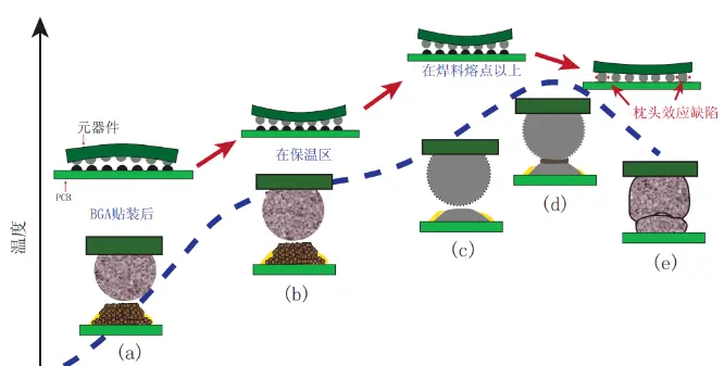
Definition: A connection point consisting of two distinctly metallurgical masses. One part is formed by the BGA solder ball, and the other part is formed by reflowed solder paste, with incomplete or no fusion between them. This defect has many other names, such as head and pillow, head in pillow, ball in cup, ball in SOCket, and hidden pillow (see Figure 3). Figure 4 illustrates the sequence of formation of the pillow effect defect.
Firstly, the BGA is placed on the printed circuit board (PCB) land coated with printed solder paste (Figure 4(a)). As the BGA on the PCB enters the reflow oven, the temperature of the BGA will rise. Due to certain factors such as packaging or/and dynamic bending of the PCB (Figure 4(b)), the gap between the solder ball and the solder paste will gradually increase. The solder on the PCB land melts, and flux covers its suRFace. At this point, the solder ball also begins to melt, but its surface typically has little or no flux coverage, and the solder ball will begin to oxidize (Figure 4(c)). When the BGA package begins to collapse, the solder ball comes into contact with the molten solder paste again. At this point, the solder ball and the molten solder paste aggregate together, and an ideal solder joint will be formed. However, if the flux activity is insufficient or the surface of the solder ball is too severely oxidized, the pillow effect will occur.
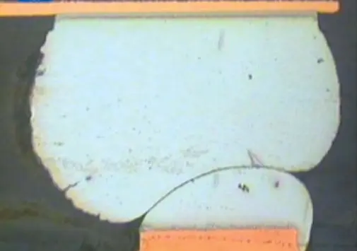
1、Dynamic Warpage: If during reflow, package warpage is caused by the mismatch in coefficient of thermal expansion (CTE) between the substrate and silicon as the package temperature rises in the oven, this warpage effect can cause some solder balls to lift away from the solder paste on the board. When flux remains on the pad and the solder ball lacks flux, this situation increases the growth of oxidation on the surface of the solder ball. Usually, when package warpage is the primary cause, HoP defects occur in the areas with the highest package warpage, and adjacent solder joints will be elongated. Figure 5 shows a severely warped BGA corner lifting up, leading to HoP. The circuit board may bend or sag during reflow, increasing the gap between the package solder balls and the solder paste. When the circuit board is thin and unsupported during reflow, board warpage becomes the primary cause of HoP. Typically, when circuit board or package warpage is the primary cause, more than one solder ball will show signs of HoP defects, and adjacent solder joints will also be elongated accordingly.
2、Reflow Profile: Due to the presence of temperature differences (dT), reflow temperature profile parameters have a significant impact on the causes of HoP defects. Due to circuit board design (copper layer distribution), laminate or package materials, and package type and size, dT can exist within a single component. Due to air flow, there can also be dT between the outer and inner rows of BGA solder balls. Generally, the temperature of the outer row of BGA solder balls is higher than that of the inner row, resulting in a delay in melting time between the outer and inner rows. However, even if they melt at different times, the collapse of the package can only occur after the inner row of solder balls also melts. This lag also exposes the outermost two rows of solder balls to high temperatures for an extended period without flux protection, leading to oxidation and thus HoP. The difference in liquefaction time between inner and outer row solder balls is called Liquid Phase Time Delay (LTD) and plays a critical role in HoP (see Figure 6). Figure 6 shows two Time-Above-Liquidus (TAL) values. However, the TAL after collapse, indicated by the shaded area, is the minimum TAL required to achieve an ideal solder joint. In other words, to minimize HoP, it is necessary to ensure that the actual TAL is sufficiently long to form a good solder joint.
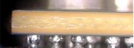
3、Solder Paste: To address the welding challenges posed by exposure to lead-free high temperatures and excessive oxidation of solder balls caused by separation from the solder paste, the properties of the solder paste are crucial. The flux chemical composition of these lead-free solders must have sufficient performance to prevent flux activity from being depleted at high temperatures. The three key properties affecting HoP defects are: the stability of the solder paste over time and temperature, the wettability of the solder paste, and the oxidation resistance of the solder paste. Solder paste with lower oxidation resistance means that the flux cannot protect the surface of the solder powder, and severe oxidation occurring on the outer surface is also known as the grape effect. Figure 7 shows the solder paste applied to the circuit board after reflow, with unfused solder particles visible, indicating that the solder paste did not have good oxidation resistance during the reflow process.
4、How to Mitigate HoP Issues: HoP is not an easy-to-solve defect, as there are many failure modes that can lead to this defect. In many cases, HoP issues are caused by multiple failure modes simultaneously. The best way to address this issue is to first identify the primary failure mode that needs to be addressed to eliminate HoP. When HoP issues are present, increasing the amount of solder paste can reduce the incidence of HoP. This may require overlay printing of solder paste on some or all lands. The reflow parameters that affect HoP are peak temperature and TAL. When dealing with HoP defects, increasing TAL and peak temperature can reduce the defect level by increasing the contact time between the package and the solder paste after the solder balls have completely collapsed and melted. Another reflow parameter that affects HoP is the soak time, whose impact depends on the type of solder paste used and its behavior in high-temperature environments. Follow the recommendations of the solder paste manufacturer and ensure that the flux should not be pressed and dried before reflow. Using nitrogen during reflow can reduce oxidation and increase SMT yield (reduce HoP).