 PCB
PCB FPC
FPC Rigid-Flex
 FR-4
FR-4 HDI PCB
 Rogers High-Frequency Board
 PTFE Teflon High-Frequency Board
 Aluminum
 Copper Core
 PCB Assembly
 LED light PCBA
 Memory PCBA
 Power Supply PCBA
 New Energey PCBA
 Communication PCBA
 Industrial Control PCBA
 Medical Equipment PCBA
 Testing Service
 PCBA Testing Service
 Certification Application
 RoHS Certification Application
 REACH Certification Application
 CE Certification Application
 FCC Certification Application
 CQC Certification Application
 UL Certification Application
 Transformers, Inductors
 High Frequency Transformers
 Low Frequency Transformers
 High Power Transformers
 Conversion Transformers
 Sealed Transformers
 Ring Transformers
 Inductors
 Wires,Cables Customized
 Network Cables
 Power Cords
 Antenna Cables
 Coaxial Cables
 Net Position Indicator
 Solar AIS net position indicator
 Capacitors
 Connectors
 Diodes
 Embedded Processors & Controllers
 Digital Signal Processors (DSP/DSC)
 Microcontrollers (MCU/MPU/SOC)
 Programmable Logic Device(CPLD/FPGA)
 Communication Modules/IoT
 Resistors
 Through Hole Resistors
 Resistor Networks, Arrays
 Potentiometers,Variable Resistors
 Aluminum Case,Porcelain Tube Resistance
 Current Sense Resistors,Shunt Resistors
 Switches
 Transistors
 Power Modules
 Isolated Power Modules
 AC-DC Power Modules
 DC-AC Module(Inverter)
 RF and Wireless
(III)What are the welding defects of SMT BGA?
SMT BGA Soldering Defects, Causes of Poor Quality, and Improvement Measures
Section Six: Ball Lift/Non-Wetting Open (NWO)
Ball lift or non-wetting open (NWO) is a common failure characteristic SIMilar to the pillowing effect, where the balls do not properly adhere to the lands, resulting in an open circuit. This failure typically occurs when the package is severely warped. During reflow soldering, the solder paste on the lands fails to remain in its intended position and instead adheres to the solder balls. Due to package warpage, a gap forms between the package solder balls and the solder paste, with the solder adhering to and fusing with the solder balls. Exposure of the PCB lands to high reflow temperatures without flux protection leads to oxide accumulation, causing the solder balls to lift and form open solder joints. Typically, no intermetallic compound (IMC) forms on these lands, and they appear as if no solder paste was ever printed on them (see Figure 8).
Factors influencing ball lift include the types of solder paste and flux, the suRFace treatment of the PCB lands (e.g., OSP), land design (SMD vs. MD), and inner-layer copper routing (thermal/ground planes). To reduce ball lift, one can alter the chemical composition of the solder paste, increase the amount of solder paste, or use nitrogen, among other solutions similar to those for Hot Press (HoP). Increasing the size of the BGA lands can also decrease the probability of ball lift, as a larger solder paste area provides greater surface tension to retain the solder paste rather than allowing the solder balls to carry it away.
Section Seven: Component Defects
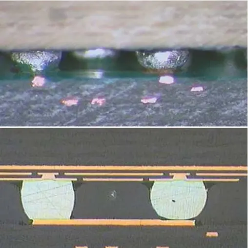
Component defects, such as popcorn effect and package warpage, are often caused by improper handling of BGA components prior to reflow soldering. Both issues produce distinct characteristic images in X-ray inspections. The popcorn effect causes the BGA package to expand underneath the chip, leading to an increase in the size of the solder balls in the center of the package (which may result in bridging), as the solder balls are flattened between the package and the circuit board (see Figure 9). BGA warpage is less noticeable than the popcorn effect and more difficult to detect in X-ray images (see Figure 10). The degree of warpage is greatest at the corners of the package, so when warpage occurs, the X-ray image of the warped BGA will show greatly elongated solder connections at the package corners. Figure 10a shows an X-ray image, and Figure 10b shows a video microscopic image of the package. It is noteworthy to observe the ripples on the substrate in Figure 10b, which are likely indicative of stress relief during reflow soldering.
Section Eight: Defect Correlation/Process Improvement
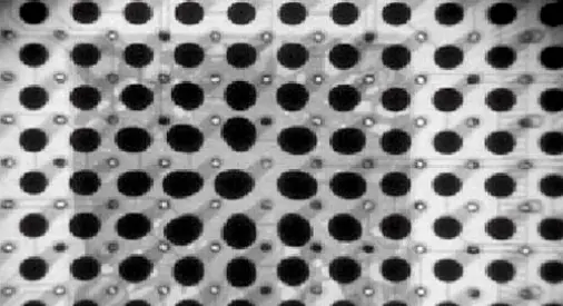
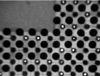
Utilizing inspection information to control manufacturing processes and maximize quality and yield is crucial. The manufacturing process leaves information on each component (acceptable or unacceptable), which can be observed through inspection. This information can be observed using methods and tools discussed previously. In many cases, visual inspection of BGAs is the first clue to any issues. Operators can examine the edges of all four sides of the BGA. The distance between the BGA and the circuit board should be uniform, and the shape of the solder balls should be consistent. To directly observe the solder connections under the BGA, X-ray or optical inspection (endoscopy) is necessary. These methods can be used to detect obvious defects such as bridging and missing solder balls. They are also useful for characterizing the BGA reflow process. During inspection, the consistency of the size and shape of the BGA solder balls should be checked. In the absence of wetting indications, the solder balls should appear round, and the entire package should have uniform dimensions. PBGA solder balls with a pre-reflow diameter of 0.75mm will expand to a nominal diameter of 0.90mm after reflow, representing a 20% increase. From the center to the edge of the package, the variation in solder ball area is typically 10-15%, but variations greater than this indicate issues with the reflow process. Inspecting the BGA with X-rays at an angle is also useful for examining the shape of the BGA solder balls in the area contacting the lands. By changing the angle of the X-ray inspection, the lands will shift, avoiding obscuring the rest of the solder balls. This allows the operator to inspect the shape of the solder connections formed on the lands to verify that the lands are in contact with the solder balls and that the solder fully wets the lands. Quantitative measurement of the X-ray images of the solder connections can be done using image analysis software. This type of software is very useful but not necessary for inspecting BGAs. The advantage of the software lies in its ability to identify and display subtle variations in size and shape of the solder connection images that are difficult for operators to observe. These small changes are process signals for assembling components and can be used to monitor and correct process defects, many of which are associated with known process issues.