 PCB
PCB FPC
FPC Rigid-Flex
 FR-4
FR-4 HDI PCB
 Rogers High-Frequency Board
 PTFE Teflon High-Frequency Board
 Aluminum
 Copper Core
 PCB Assembly
 LED light PCBA
 Memory PCBA
 Power Supply PCBA
 New Energey PCBA
 Communication PCBA
 Industrial Control PCBA
 Medical Equipment PCBA
 Testing Service
 PCBA Testing Service
 Certification Application
 RoHS Certification Application
 REACH Certification Application
 CE Certification Application
 FCC Certification Application
 CQC Certification Application
 UL Certification Application
 Transformers, Inductors
 High Frequency Transformers
 Low Frequency Transformers
 High Power Transformers
 Conversion Transformers
 Sealed Transformers
 Ring Transformers
 Inductors
 Wires,Cables Customized
 Network Cables
 Power Cords
 Antenna Cables
 Coaxial Cables
 Net Position Indicator
 Solar AIS net position indicator
 Capacitors
 Connectors
 Diodes
 Embedded Processors & Controllers
 Digital Signal Processors (DSP/DSC)
 Microcontrollers (MCU/MPU/SOC)
 Programmable Logic Device(CPLD/FPGA)
 Communication Modules/IoT
 Resistors
 Through Hole Resistors
 Resistor Networks, Arrays
 Potentiometers,Variable Resistors
 Aluminum Case,Porcelain Tube Resistance
 Current Sense Resistors,Shunt Resistors
 Switches
 Transistors
 Power Modules
 Isolated Power Modules
 AC-DC Power Modules
 DC-AC Module(Inverter)
 RF and Wireless
Decoupling Capacitor Quantity and Placement in Simple Power Distribution Network (PDN) Design
2025-12-18
The Power Distribution Network (PDN) serves as the "energy backbone" of electronic systems, responsible for delivering stable, low-noise power from the voltage regulator module (VRM) to all active components (such as microcontrollers, FPGAs, and analog ICs). In SIMple PDN designs—typical of consumer electronics, low-power industrial controllers, and embedded systems—decoupling capacitors are the most cost-effective and critical components for mitigating power integrity (PI) issues. They suppress voltage fluctuations (ripple), filter high-frequency noise, and provide instantaneous current demands that the VRM cannot supply in time. However, the effectiveness of decoupling capacitors is not determined by their value alone; theirquantity and placementdirectly dictate PDN peRFormance. Poorly sized or misplaced decoupling capacitors can lead to signal integrity (SI) degradation, component malfunctions, or even system failure. This article provides a comprehensive, step-by-step guide to determining the quantity and placement of decoupling capacitors in simple PDN designs, aligning with industry standards (IPC-2221, IEEE 1149.1) and practical engineering best practices. It covers the fundamental role of decoupling capacitors, key factors influencing quantity selection, placement guidelines, validation methods, and common pitfalls to avoid.
1. Fundamental Role of Decoupling Capacitors in Simple PDNs
To understand how to select and place decoupling capacitors, it is first essential to grasp their core functions in a PDN. A simple PDN typically consists of a VRM, power planes (or copper traces), load components, and decoupling capacitors. The primary challenges it faces are voltage ripple (periodic fluctuations caused by VRM switching and load current changes) and transient voltage droop (sudden voltage drops when components demand instantaneous peak current). Decoupling capacitors address these issues through three key mechanisms:
1.1 Energy Storage and Transient Current Supply
Active components (e.g., a microcontroller executing an instruction) require rapid, short-duration current pulses (transient current). VRMs, due to their inherent inductance and switching delay, cannot respond instantaneously to these demands. Decoupling capacitors act as "local energy reservoirs," storing charge and supplying the required transient current directly to the component’s power pins. This eliminates voltage droop that would otherwise occur if the current had to travel from the VRM through long, inductive traces.
1.2 High-Frequency Noise Filtering
Power traces and planes act as transmission lines, propagating high-frequency noise generated by switching components (e.g., MOSFETs in the VRM or digital ICs). Decoupling capacitors shunt this high-frequency noise to ground, preventing it from interfering with sensitive components (such as analog-to-digital converters or radio modules). The effectiveness of this filtering depends on the capacitor’s parasitic parameters (equivalent series resistance, ESR; equivalent series inductance, ESL) and its proximity to the noise source.
1.3 Voltage Ripple Suppression
Even well-regulated VRMs produce small voltage ripples at their switching frequency (typically 100 kHz–2 MHz). Decoupling capacitors, especially those with low ESR (e.g., ceramic capacitors), dampen these ripples by providing a low-impedance path for alternating current (AC) components of the load current. This ensures that the voltage supplied to the component remains within its specified tolerance (e.g., ±5% for a 3.3V power rail).
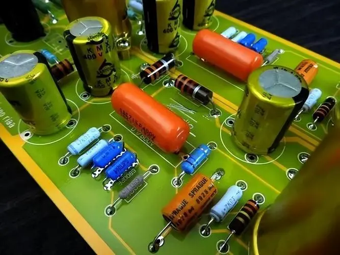
In simple PDNs, where power rails are relatively low-current (≤10A) and operating frequencies are moderate (≤1 GHz), ceramic capacitors (X5R, X7R dielectrics) are the primary choice for decoupling due to their low ESR, low ESL, and high capacitance density. Tantalum or aluminum electrolytic capacitors may be used as "bulk" decoupling to complement ceramic capacitors for lower-frequency ripple suppression.
2. Determining the Quantity of Decoupling Capacitors
The quantity of decoupling capacitors required in a simple PDN is determined by four core factors: the load’s transient current demand, the capacitor’s parasitic parameters (ESR/ESL), the allowable voltage ripple, and the number of power pins on the load component. There is no "one-size-fits-all" formula, but a systematic approach combining calculation, simulation, and industry guidelines ensures optimal sizing.
2.1 Key Input Parameters for Quantity Calculation
Before calculating the number of decoupling capacitors, the following parameters must be defined based on the component datasheet and system requirements:
- Maximum Transient Current (I): The peak current demanded by the component during operation (e.g., 2A for a microcontroller during a DMA transfer). This is typically specified in the component’s electrical characteristics datasheet.
- Allowable Voltage Droop (ΔV): The maximum acceptable voltage drop on the power rail during a transient event. This is usually 3–5% of the nominal voltage (e.g., 0.165V for a 3.3V rail).
- Transient Duration (Δt): The length of time the transient current is drawn (e.g., 10 ns for a high-speed logic transition). This can be estimated from the component’s switching frequency (Δt ≈ 1/(2×f)).
- Capacitor Parameters: For the selected capacitor (e.g., 0402 X7R 1μF 6.3V), the ESR (R, typically 5–50 mΩ) and capacitance (C) are critical. The ESL (L, typically 0.5–2 nH) is also important for high-frequency performance.
- Number of Power Pins (N): Each power pin on the load component should have dedicated decoupling, as current distribution across multiple pins is non-uniform. A minimum of one decoupling capacitor per power pin is a common starting point.
2.2 Calculation Methodology for Decoupling Capacitance
The total decoupling capacitance (C) required to suppress transient voltage droop is derived from the energy storage principle: the energy stored in the capacitors must be sufficient to supply the transient current demand during Δt, while accounting for voltage droop. The basic formula is:
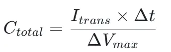
This formula assumes ideal capacitors (zero ESR/ESL). However, real capacitors have parasitic resistance, which contributes additional voltage droop. The total voltage droop in a real PDN is the sum of the droop from capacitance discharge (ΔV) and the droop from ESR (ΔV):
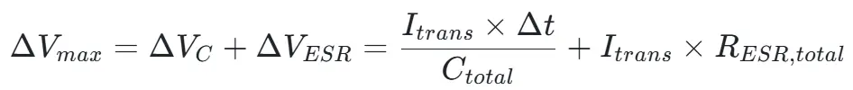
Where R is the total ESR of the decoupling capacitor bank. For N identical capacitors in parallel, R = R/N, and C = N × C.
Rearranging to solve for N (number of capacitors):
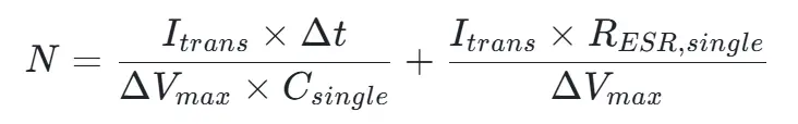
2.3 Example Calculation
Consider a simple PDN powering a 3.3V microcontroller with the following parameters:
- Nominal voltage (V): 3.3V
- Allowable voltage droop (ΔV): 5% of 3.3V = 0.165V
- Maximum transient current (I): 1.5A
- Transient duration (Δt): 20 ns (switching frequency = 25 MHz)
- Selected capacitor: 0603 X7R 1μF 6.3V, R = 20 mΩ, C = 1μF
Substituting into the formula:
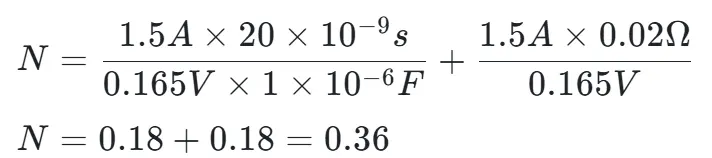
Since the number of capacitors cannot be fractional, we round up to N = 1. However, this is a minimum value. Additional factors (such as ESL, trace inductance, and multiple power pins) typically require increasing the quantity. If the microcontroller has 4 power pins, a practical approach would be 4 capacitors (one per pin) to ensure uniform current distribution.
2.4 Guidelines for Quantity Selection in Simple PDNs
For simple PDNs (low current, moderate frequency), the following industry guidelines complement the calculation method to determine the number of decoupling capacitors:
- Per-Pin Decoupling: Assign at least one decoupling capacitor (0.1μF or 1μF ceramic) to each power pin of the load component. This ensures that each pin has a local energy source, minimizing current sharing issues across pins.
- Bulk Decoupling Complement: Add 1–2 bulk decoupling capacitors (10μF–100μF tantalum or aluminum electrolytic) per power rail. These handle lower-frequency ripple (100 kHz–1 MHz) and replenish the charge in the ceramic decoupling capacitors.
- Frequency-Dependent Sizing: For components with switching frequencies above 500 MHz, use a combination of capacitor values (e.g., 1μF, 0.1μF, 0.01μF) to cover a wider frequency range. Each value addresses a specific frequency band: 1μF for low frequencies (100 kHz–1 MHz), 0.1μF for mid-frequencies (1–10 MHz), and 0.01μF for high frequencies (10–100 MHz).
- Current-Based Sizing: For power rails with current demands above 1A, add one additional 1μF ceramic capacitor for every 1A of current. For example, a 3A rail would require 3–4 1μF capacitors plus bulk decoupling.
- Derating Factor: Apply a 20–30% derating factor to the calculated capacitance to account for temperature effects (X5R/X7R dielectrics lose capacitance at extreme temperatures) and manufacturing tolerance (±10% for X7R).
3. Determining the Placement of Decoupling Capacitors
In PDN design, "placement is everything"—a well-sized decoupling capacitor bank will fail to perform if the capacitors are not placed correctly. The primary goal of placement is to minimize the inductance of the path between the capacitor and the component’s power pin (the "decoupling loop"). Inductance (from traces, vias, and capacitor pads) reduces the capacitor’s ability to supply transient current at high frequencies. Key placement guidelines for simple PDNs are outlined below, organized by critical design principles.
3.1 Minimize the Decoupling Loop Inductance
The decoupling loop consists of the path from the component’s power pin, through the decoupling capacitor, to the ground pin. The inductance of this loop (L) is the primary limiting factor for high-frequency performance. To minimize L:
- Place Capacitors as Close as Possible to Power Pins: The ideal distance between a decoupling capacitor and the component’s power pin is ≤2mm. For every 1mm increase in distance, the loop inductance increases by approximately 1 nH, which can reduce the capacitor’s effectiveness at frequencies above 100 MHz. For fine-pitch components (e.g., QFP, BGA), place capacitors between the component’s pins or on the opposite side of the PCB (directly below the power pins) using vias.
- Use Short, Wide Traces: Traces connecting the capacitor to the power pin should be as short and wide as possible. Wide traces (≥0.8mm for 3.3V rails) reduce resistance and inductance. Avoid narrow traces or long, meandering paths, which act as high-impedance transmission lines at high frequencies.
- Minimize the Number of Vias: Vias introduce significant inductance (≈0.5–1 nH per via). If capacitors must be placed on the opposite side of the PCB, use a single via for the power connection and a single via for the ground connection, placed as close to the capacitor pads as possible. Avoid "stitching" vias (multiple vias in series), which multiply inductance.
- Use Power/Ground Plane Pairs: In multi-layer PCBs, use adjacent power and ground planes to form a low-inductance transmission line. The capacitor can be connected directly to these planes using short vias, minimizing the loop inductance. For two-layer PCBs (common in simple PDNs), use large ground copper pours adjacent to the power trace to reduce loop area.
3.2 Optimize Ground Connection
The ground connection of the decoupling capacitor is as critical as the power connection, as the ground path forms half of the decoupling loop. Poor ground placement can create ground bounce (voltage fluctuations on the ground plane), which degrades both PI and SI. Guidelines for ground placement:
- Connect Capacitor Ground to Component Ground Pin: The capacitor’s ground terminal should be connected directly to the component’s ground pin, either via a short trace or a ground plane. Avoid connecting the capacitor to a distant ground node, as this increases the loop inductance and introduces ground bounce.
- Use a Single Ground Point for Decoupling Capacitors: For multiple decoupling capacitors associated with a single component, connect their ground terminals to a common ground point near the component’s ground pins. This creates a "star" ground configuration, minimizing cross-talk between capacitors.
- Avoid Ground Plane Splits: In two-layer PCBs, avoid splitting the ground plane (e.g., separating analog and digital ground with a trace), as this forces the decoupling current to flow around the split, increasing loop inductance. If splits are necessary, use a single ground plane with controlled impedance bridges.
3.3 Separate Decoupling Capacitor Types by Function
Different types of decoupling capacitors (ceramic, tantalum, electrolytic) serve different frequency ranges and should be placed accordingly to avoid interference:
- Ceramic Capacitors (High-Frequency Decoupling): Place ceramic capacitors (0.01μF–1μF) directly adjacent to the component’s power pins, as they handle high-frequency transient currents (1 MHz–100 MHz).
- Bulk Capacitors (Low-Frequency Decoupling): Place bulk capacitors (10μF–100μF) near the VRM or along the main power rail, as they handle low-frequency ripple (100 kHz–1 MHz) and replenish the ceramic capacitors. Bulk capacitors do not need to be as close to the load component, as their performance is less sensitive to inductance.
- Analog vs. Digital Decoupling: For systems with both analog and digital components, separate their decoupling capacitors to prevent digital noise from coupling into analog circuits. Place analog decoupling capacitors near analog power pins, connected to an analog ground plane (if available), and digital decoupling capacitors near digital power pins.
3.4 Placement for Multi-Component PDNs
In simple PDNs with multiple load components (e.g., a microcontroller, a sensor, and a communication module), each component should have its own dedicated decoupling capacitors. Additionally:
- Distribute Bulk Capacitors Along the Power Rail: Place bulk capacitors every 2–3 inches (50–75mm) along the main power rail to ensure uniform voltage distribution across the PCB.
- Avoid Overlapping Decoupling Loops: Arrange decoupling capacitors such that their loops (power pin → capacitor → ground pin) do not overlap. Overlapping loops can cause electromagnetic coupling between capacitors, increasing noise.
- Prioritize Critical Components: Place higher-performance decoupling capacitors (lower ESR/ESL) near critical components (e.g., a radio module with strict noise requirements) and standard capacitors near less sensitive components (e.g., a voltage reference).
4. Validation and Optimization of Decoupling Capacitor Quantity and Placement
After determining the initial quantity and placement of decoupling capacitors, validation is essential to ensure the PDN meets performance requirements. For simple PDNs, validation can be performed using a combination of simulation, measurement, and visual inspection.
4.1 Simulation Tools for PDN Analysis
Simple PDN simulation tools (e.g., Altium Designer’s PDN Analyzer, Cadence Allegro PDN Analyst) can predict voltage ripple, transient droop, and impedance across the power rail. Key simulation steps:
- Model the PDN components: VRM (using a Thevenin equivalent), power traces/plane (using impedance models), load components (using current-source models), and decoupling capacitors (including ESR/ESL).
- Simulate transient conditions: Apply the maximum transient current to the load and measure the voltage droop. If the droop exceeds ΔV, increase the number of decoupling capacitors or optimize their placement.
- Simulate impedance vs. frequency: The PDN’s target impedance (Z) is defined as ΔV/I. The simulation should confirm that the PDN’s impedance is below Z across the component’s operating frequency range. If impedance is too high at a specific frequency, add a decoupling capacitor of the appropriate value to resonate at that frequency.
4.2 Physical Measurement and Testing
For prototype PCBs, physical measurements validate simulation results. Key tests include:
- Voltage Ripple Measurement: Use an oscilloscope with a high-bandwidth probe (≥100 MHz) to measure voltage ripple at the component’s power pin. The ripple amplitude should be below the allowable limit (e.g., 50 mV for a 3.3V rail).
- Transient Voltage Droop Measurement: Trigger the oscilloscope on the component’s transient event (e.g., a DMA transfer) and measure the voltage droop. If the droop is excessive, add more decoupling capacitors or move existing capacitors closer to the power pin.
- Impedance Measurement: Use a network analyzer to measure the PDN’s impedance at the component’s power pin. Compare the measurement to the target impedance to identify frequency bands where additional decoupling is needed.
4.3 Visual Inspection for Placement Errors
Visual inspection of the PCB (using a digital microscope) identifies placement issues that can degrade PDN performance:
- Decoupling capacitors are placed more than 2mm from the power pin.
- Traces between capacitors and power pins are narrow or meandering.
- Excessive vias are used in the decoupling loop.
- Ground connections are not directly linked to the component’s ground pin.
5. Common Pitfalls to Avoid in Decoupling Capacitor Design
Even experienced engineers can make mistakes in decoupling capacitor quantity and placement. The following are common pitfalls and their solutions:
5.1 Over-Capacitating the PDN
Adding more decoupling capacitors than necessary increases cost, PCB space, and VRM inrush current (the current required to charge the capacitors when the system powers on). Solution: Use simulation to determine the minimum number of capacitors needed to meet ΔV and Z requirements.
5.2 Using Capacitors with High ESR/ESL
Low-quality capacitors (e.g., Y5V dielectrics) have high ESR and ESL, reducing their decoupling effectiveness. Solution: Select ceramic capacitors with X5R or X7R dielectrics, which have low ESR (≤50 mΩ) and stable capacitance over temperature.
5.3 Placing All Capacitors on One Side of the PCB
For BGA or QFP components, placing all decoupling capacitors on the top side (away from the power pins) increases loop inductance. Solution: Use a multi-layer PCB and place capacitors on the bottom side, directly below the power pins, with short vias.
5.4 Ignoring Trace Inductance in Two-Layer PCBs
Two-layer PCBs lack dedicated power/ground planes, making trace inductance a major issue. Solution: Use large ground copper pours adjacent to power traces, minimize trace length, and use wider traces (≥1mm) for high-current paths.
5.5 Using a Single Large Capacitor Instead of Multiple Small Ones
A single 10μF capacitor has higher ESL than ten 1μF capacitors in parallel (ESL scales with 1/N for N parallel capacitors). Solution: Use multiple small capacitors in parallel to reduce total ESL and improve high-frequency performance.
6. Conclusion
In simple PDN design, the quantity and placement of decoupling capacitors are critical determinants of power integrity. The quantity is determined by the load’s transient current demand, allowable voltage droop, and capacitor parasitic parameters, with guidelines such as per-pin decoupling and bulk capacitor complement ensuring practical implementation. Placement focuses on minimizing the decoupling loop inductance through close proximity to power pins, short wide traces, and optimized ground connections. Validation through simulation and physical measurement ensures that the PDN meets performance requirements, while avoiding common pitfalls (over-capacitation, high ESR capacitors) further enhances reliability.