 PCB
PCB FPC
FPC Rigid-Flex
 FR-4
FR-4 HDI PCB
 Rogers High-Frequency Board
 PTFE Teflon High-Frequency Board
 Aluminum
 Copper Core
 PCB Assembly
 LED light PCBA
 Memory PCBA
 Power Supply PCBA
 New Energey PCBA
 Communication PCBA
 Industrial Control PCBA
 Medical Equipment PCBA
 Testing Service
 PCBA Testing Service
 Certification Application
 RoHS Certification Application
 REACH Certification Application
 CE Certification Application
 FCC Certification Application
 CQC Certification Application
 UL Certification Application
 Transformers, Inductors
 High Frequency Transformers
 Low Frequency Transformers
 High Power Transformers
 Conversion Transformers
 Sealed Transformers
 Ring Transformers
 Inductors
 Wires,Cables Customized
 Network Cables
 Power Cords
 Antenna Cables
 Coaxial Cables
 Net Position Indicator
 Solar AIS net position indicator
 Capacitors
 Connectors
 Diodes
 Embedded Processors & Controllers
 Digital Signal Processors (DSP/DSC)
 Microcontrollers (MCU/MPU/SOC)
 Programmable Logic Device(CPLD/FPGA)
 Communication Modules/IoT
 Resistors
 Through Hole Resistors
 Resistor Networks, Arrays
 Potentiometers,Variable Resistors
 Aluminum Case,Porcelain Tube Resistance
 Current Sense Resistors,Shunt Resistors
 Switches
 Transistors
 Power Modules
 Isolated Power Modules
 AC-DC Power Modules
 DC-AC Module(Inverter)
 RF and Wireless
Seed Layer Selective Etching Control in mSAP Manufacturing
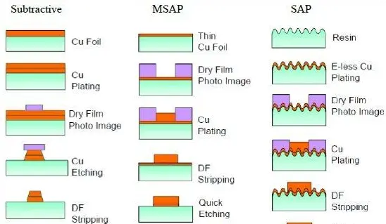
Introduction
The modified Semi-Additive Process (mSAP), critical for HDI PCB fabrication, achieves 5/5μm line/space through ultrathin seed layer plating and selective etching. Uniformity and selectivity in seed layer etching directly determine line wall profiles, suRFace roughness, and impedance consistency.
1. Seed Layer Materials and Etching Mechanisms
1.1 Typical Seed Layer Structure (Figure 1)
mSAP uses bilayer stacks:
-
Barrier layer: 10-20nm Ti/TiN to prevent copper diffusion;
-
Conductive layer: 100-200nm Cu for electroplating.
1.2 Selective Etching Chemistry
Two-step etching:
-
Cu etchant: H2SO4-H2O2 system with >100:1 selectivity (Cu vs. Ti):
-
Ti etchant: HF-HNO3 mixture with >500:1 selectivity (Ti vs. Cu):
2. Key Process Parameters
2.1 Copper Etching Control
-
Concentration management:
-
Maintain 8-12wt% H2O2 to prevent Cu+ accumulation;
-
Temperature control at 30±2℃ (25% rate increase per 5℃ rise);
-
-
Flow design:
-
Fan nozzles with 0.15-0.25MPa pressure ensure ≤±5% film uniformity.
-
2.2 Titanium Residue Prevention
-
Endpoint detection:
-
In-situ EIS monitors Ti layer resistance (±1nm accuracy);
-
-
Post-clean:
-
DIW + 40kHz ultrasonic cleaning removes H2TiF6 residues.
-
3. Defect Analysis and Solutions
3.1 Undercut Suppression
-
Issue: Excessive lateral etching (>0.3μm);
-
Solutions:
-
Add 0.5-1.0g/L benzotriazole (BTA) as inhibitor;
-
Reduce flow velocity to 0.8m/s to minimize turbulence.
-
3.2 Seed Layer Residue Control
-
Issue: Incomplete Ti etching causing shorts;
-
Solutions:
-
Increase agitation (500-600rpm) for better mass transfer;
-
Plasma ashing pre-treatment removes carbonized photoresist.
-
4. Equipment and Monitoring
4.1 Vertical Continuous Processing (VCP) Tool
-
Multi-chamber design: Cu etch → rinse → Ti etch → rinse → dry (cycle time ≤3min);
-
Auto-dosing: ORP sensors regulate H2O2 concentration (±0.5% variation).
4.2 In-line Metrology
-
Optical interferometer: Measures seed layer thickness (±2nm);
-
XRF spectrometer: Detects metal residues (<10ppm detection limit).
5. Case Study: IC Substrate Parameters
-
Cu seed layer: 150nm;
-
Etch uniformity: Within-wafer (WIW) ≤3%, wafer-to-wafer (WTW) ≤5%;
-
Line sidewall angle: 88±2° (target 90°);
-
Impedance control: ±5% deviation at 10GHz.