 PCB
PCB FPC
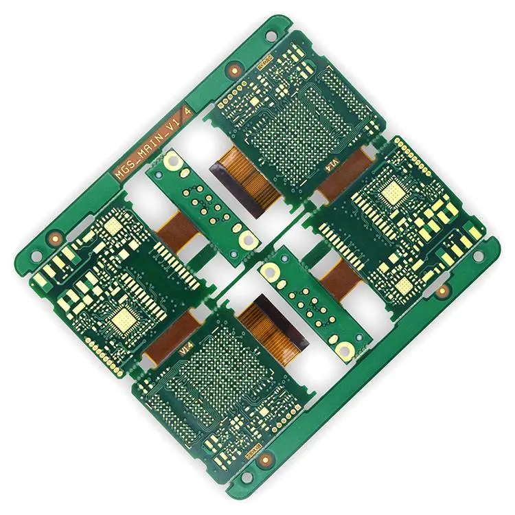
FPC Rigid-Flex
 FR-4
FR-4 HDI PCB
 Rogers High-Frequency Board
 PTFE Teflon High-Frequency Board
 Aluminum
 Copper Core
 PCB Assembly
 LED light PCBA
 Memory PCBA
 Power Supply PCBA
 New Energey PCBA
 Communication PCBA
 Industrial Control PCBA
 Medical Equipment PCBA
 Testing Service
 PCBA Testing Service
 Certification Application
 RoHS Certification Application
 REACH Certification Application
 CE Certification Application
 FCC Certification Application
 CQC Certification Application
 UL Certification Application
 Transformers, Inductors
 High Frequency Transformers
 Low Frequency Transformers
 High Power Transformers
 Conversion Transformers
 Sealed Transformers
 Ring Transformers
 Inductors
 Wires,Cables Customized
 Network Cables
 Power Cords
 Antenna Cables
 Coaxial Cables
 Net Position Indicator
 Solar AIS net position indicator
 Capacitors
 Connectors
 Diodes
 Embedded Processors & Controllers
 Digital Signal Processors (DSP/DSC)
 Microcontrollers (MCU/MPU/SOC)
 Programmable Logic Device(CPLD/FPGA)
 Communication Modules/IoT
 Resistors
 Through Hole Resistors
 Resistor Networks, Arrays
 Potentiometers,Variable Resistors
 Aluminum Case,Porcelain Tube Resistance
 Current Sense Resistors,Shunt Resistors
 Switches
 Transistors
 Power Modules
 Isolated Power Modules
 AC-DC Power Modules
 DC-AC Module(Inverter)
 RF and Wireless
Rigid-Flex PCB Stack-up Design
📚 BasIC Concepts and Design Challenges
Rigid-Flex PCBs combine rigid Circuit Boards and flexible circuit boards through multiple lamination processes into a composite structure. Their core advantage lies in integrating the stability of rigid circuits with the malleability of flexible circuits, enabling high-density interconnections and three-dimensional routing.
Excessive difference in layer count between flexible and rigid areas introduces several challenges:
-
Z-axis CTE Mismatch: During hot pressing, differences in resin content and glass transition temperature between rigid materials (e.g., FR-4) and flexible materials (e.g., Polyimide) lead to varying Z-axis expansion rates, easily causing defects like delamination and blistering.
-
Stress Concentration in Bend Areas: The step groove formed by the layer count difference becomes a stress concentration point during bending. Research indicates the stress peak here can be 3-5 times the average stress, making it the primary cause of flexible circuit fatigue fracture.
-
Difficulty in Lamination Filling: When the layer difference is ≥4 layers, the thickness gap that the prepreg needs to fill during lamination exceeds 100µm, easily leading to issues like uneven resin flow and voids.
📊 Analysis of Allowable Layer Difference
The maximum allowable layer difference in Rigid-Flex boards is not a fixed value but a reflection of material properties, application scenarios, and process capabilities.
Recommended Layer Differences for Different Application Scenarios
| Application Scenario | Typical Layer Difference | Rationale & Case Support |
|---|---|---|
| Consumer Electronics (e.g., foldable phones) | Flexible area typically 2 layers; difference with rigid area recommended ≤4 layers | Uses ultra-thin copper foil (9µm) and adhesiveless materials to improve bending life; rigid area up to 6 layers for slim profile. |
| Industrial Control | Difference can reach 6-8 layers | Balances mechanical strength with certain bending requirements; uses stepped structures in transition zones to relieve stress. |
| Aerospace | Difference typically ≤4 layers | Meets vibration resistance and high reliability; uses symmetrical stack-up to balance stress and prevent warping. |
| Medical Devices (e.g., endoscopes) | Difference mostly controlled within 2-4 layers | Flexible area often 2 layers to ensure small bend radius; transmits high-speed image signals. |
Critical Parameters and Experimental Research
Research on a 6-layer Rigid-Flex board showed a clear mathematical relationship between the flexible area embedment size dE, the distance from the rigid-flex interconnect blind via to the combination edge dH, and the board's flexure count Y, expressed by the fitted equation:
Y = -34.2 + 22.7dE + 16.3dH
The study indicated that dE = 2.0 cm and dH = 1.8 cm were the minimum critical parameters satisfying the requirement of 4000 flexural cycles for the 6-layer Rigid-Flex board. This highlights the importance of precisely calculating transition zone dimensions during design for reliability.
💡 Key Design Techniques for Handling Large Layer Differences
When your design requires a significant layer count difference, the following techniques are crucial:
-
Optimize Transition Zone Design
-
Adopt a stepped thickness transition structure, which can effectively buffer bending forces, prevent damage to the flexible board at the notch, and increase the flex cycle count.
-
Fill the steps with elastic buffer gel (e.g., polyurethane or silicone) to absorb stress. Experiments show suitable buffer layers can reduce the stress peak by about 30%.
-
The circuit direction in the transition zone should be perpendicular to the bend direction, and vias should be avoided in this area.
-
-
Strictly Control Bend Radius
-
Ensure the minimum bend radius for the flexible section is maintained. Typically, for dynamic bending (repeated flexing), the radius should be ≥ 10 times the board thickness; for static bending (fixed after installation), the radius should be ≥ 6 times the board thickness.
-
For example, a 0.2mm thick 4-layer flexible board in a dynamic application should have a bend radius no less than 2mm.
-
-
Material Selection and Stack-up Strategy
-
Adhesiveless, rolled annealed polyimide substrates are recommended for the flexible parts. Compared to adhesive materials, their flex endurance can be improved by about 50%, and they offer better dimensional stability.
-
Employ a symmetrical stack-up structure (e.g., Flex | Cu | Rigid Core | Cu | Flex) to help balance stress and prevent board warpage.
-
Consider using thinner copper foils (e.g., 9μm or 12μm) in the flexible areas to enhance their flexibility.
-
-
Precision Trace and Via Handling
-
Traces in flexible areas should avoid sudden widening or narrowing, using teardrop transitions; independent pads can be reinforced with panel toes for better support.
-
Vias in flexible areas are susceptible to stress due to repeated bending. It is advisable to prioritize laser blind or buried vias and avoid placing vias in severe bending areas. If through-holes are necessary, their diameter should be ≤0.2mm.
-
💎 Summary and Best Practices
The layer count design for Rigid-Flex PCBs is an art of balance. The key points are summarized as follows:
-
There is no absolute upper limit for layer difference, but it is constrained by reliability requirements. For dynamic bending consumer products, a difference of ≤4 layers is recommended; for industrial and special scenarios, it can be extended to 6-8 layers, but must be supported by reinforced design.
-
Transition zone design is core. Referencing empirical formulas and critical parameters, using stepped transitions and buffer materials is key to managing stress concentration.
-
Adhere to bend radius and routing rules. Ensure the bend radius is ≥ 6-10 times the board thickness, and the trace direction is perpendicular to the bend direction.
-
Material selection determines the performance baseline. Prioritize high-performance flexible materials like adhesiveless, rolled annealed types to lay a solid foundation for high-density stack-ups.
The best design strategy is to work closely with your PCB manufacturer from the early stages of the project to evaluate and determine the most suitable stack-up based on specific product requirements.