 PCB
PCB FPC
FPC Rigid-Flex
 FR-4
FR-4 HDI PCB
 Rogers High-Frequency Board
 PTFE Teflon High-Frequency Board
 Aluminum
 Copper Core
 PCB Assembly
 LED light PCBA
 Memory PCBA
 Power Supply PCBA
 New Energey PCBA
 Communication PCBA
 Industrial Control PCBA
 Medical Equipment PCBA
 Testing Service
 PCBA Testing Service
 Certification Application
 RoHS Certification Application
 REACH Certification Application
 CE Certification Application
 FCC Certification Application
 CQC Certification Application
 UL Certification Application
 Transformers, Inductors
 High Frequency Transformers
 Low Frequency Transformers
 High Power Transformers
 Conversion Transformers
 Sealed Transformers
 Ring Transformers
 Inductors
 Wires,Cables Customized
 Network Cables
 Power Cords
 Antenna Cables
 Coaxial Cables
 Net Position Indicator
 Solar AIS net position indicator
 Capacitors
 Connectors
 Diodes
 Embedded Processors & Controllers
 Digital Signal Processors (DSP/DSC)
 Microcontrollers (MCU/MPU/SOC)
 Programmable Logic Device(CPLD/FPGA)
 Communication Modules/IoT
 Resistors
 Through Hole Resistors
 Resistor Networks, Arrays
 Potentiometers,Variable Resistors
 Aluminum Case,Porcelain Tube Resistance
 Current Sense Resistors,Shunt Resistors
 Switches
 Transistors
 Power Modules
 Isolated Power Modules
 AC-DC Power Modules
 DC-AC Module(Inverter)
 RF and Wireless
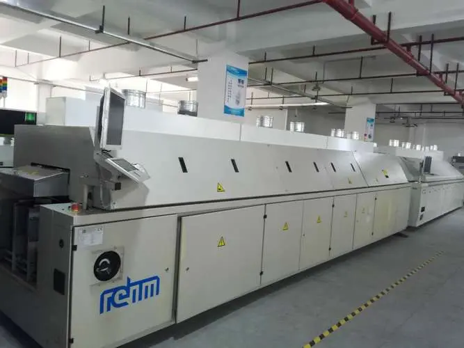
Reflow Oven Profile Parameters for Conventional Sn-Pb Solder: A Comprehensive Guide to Preheat, Soak, Reflow and Cooling Zones
2025-12-12
Conventional tin-lead (Sn-Pb) solder, most commonly in the 63Sn-37Pb eutectIC formulation, has long been a staple in electronic assembly due to its low melting point (183°C), excellent wetting properties, and reliable solder joint formation. Despite the global shift toward lead-free alternatives for environmental compliance, Sn-Pb solder remains widely used in high-reliability applications such as aerospace, military electronics, and precision medical devices, where its predictable melting behavior and superior fatigue resistance are critical. The key to achieving consistent, defect-free solder joints with Sn-Pb solder lies in optimizing the reflow oven temperature profile—a sequence of precisely controlled heating and cooling stages that includes preheat, soak, reflow, and cooling zones. This article provides a detailed analysis of the temperature, time, and ramp rate parameters for each zone, aligned with industry standards (IPC/JEDEC J-STD-020), and explains how these parameters influence solder joint quality, component reliability, and manufacturing yield.
1. Fundamentals of Sn-Pb Solder Reflow: Key Principles and Quality Drivers
Before diving into zone-specific parameters, it is essential to understand the core chemical and physical processes that occur during Sn-Pb reflow, as these processes dictate the constraints for temperature and time settings.
1.1 Eutectic Properties of 63Sn-37Pb Solder
The 63Sn-37Pb alloy is a eutectic mixture, meaning it transitions directly from a solid to a liquid state at a single, well-defined temperature of 183°C—no pasty phase (a mixture of solid and liquid solder) exists during melting. This unique property is a major advantage of Sn-Pb solder: it eliminates the risk of component movement (tombstoning) during reflow, as the solder melts and solidifies rapidly. For successful reflow, the solder paste must be heated above 183°C to fully liquefy, allowing it to wet the component leads and PCB pads, then cooled at a controlled rate to form a solid, metallurgically sound joint.
1.2 Critical Reflow Profile Metrics
A valid Sn-Pb reflow profile is defined by five key metrics, as specified in IPC/JEDEC J-STD-020:
- Ramp Rate: The rate of temperature increase (or decrease) between zones, measured in °C/second (°C/s). Excessively fast ramp rates cause thermal shock, while slow ramp rates lead to solder paste oxidation.
- Preheat Temperature Range: The temperature range (typically 120–150°C) where solder paste solvents evaporate and flux activates.
- Soak Time: The duration the PCB is held in the preheat range to ensure uniform temperature across all components.
- Peak Temperature: The maximum temperature the PCB reaches during reflow, typically 200–220°C (17–37°C above the eutectic point).
- Time Above Liquidus (TAL): The duration the solder remains in the liquid state (above 183°C), typically 30–60 seconds.
Deviations from these metrics can cause a range of defects, including insufficient wetting, solder balls, pad lifting, and component damage.
1.3 Component and PCB Thermal Constraints
The reflow profile must also account for the thermal limits of components and Pcb Materials to prevent damage:
- Sensitive Components: Electrolytic Capacitors, plastic ICs, and LEDs typically have a maximum peak temperature limit of 220°C and a maximum ramp rate of 2°C/s.
- PCB Substrates: Standard FR-4 PCBs have a glass transition temperature (Tg) of 120–140°C; prolonged exposure to temperatures above Tg can cause warping or delamination.
- Thermal Mass Variation: Large components (e.g., connectors, transformers) have higher thermal mass than small components (e.g., resistors, capacitors), requiring a longer soak time to ensure uniform heating across the PCB.
2. Zone-by-Zone Reflow Oven Parameters for Sn-Pb Solder
A typical reflow oven consists of 4–8 heating zones (divided into preheat, soak, and reflow sections) followed by 1–2 cooling zones. Each zone has distinct temperature, time, and ramp rate parameters tailored to the Sn-Pb reflow process.
2.1 Preheat Zone: Solvent Evaporation and Flux Activation
The preheat zone is the first stage of the reflow process, where the PCB temperature is gradually increased from room temperature (25°C) to the soak temperature range (120–150°C). The primary goals of this zone are to evaporate volatile solvents in the solder paste and activate the flux, which removes oxide layers from component leads and PCB pads to enable solder wetting.
Key Parameters for Preheat Zone
- Temperature Range: 120–150°C (measured at the PCB surface)
- Ramp Rate: 0.5–2.0°C/s (maximum 2.5°C/s for Sn-Pb solder, per IPC/JEDEC J-STD-020)
- Total Preheat Time: 60–120 seconds (varies based on PCB thermal mass)
- Temperature Uniformity: ±5°C across the PCB surface
Parameter Justification and Defect Prevention
- Ramp Rate Control: A ramp rate below 0.5°C/s is inefficient and can cause excessive flux oxidation, while a rate above 2.5°C/s leads to thermal shock. Thermal shock can crack ceramic components (e.g., MLCCs) or delaminate plastic IC packages, as different materials expand at different rates.
- Temperature Range Limits: Temperatures below 120°C are insufficient to activate the flux, leading to poor wetting and solder balls. Temperatures above 150°C can cause the flux to burn out prematurely, leaving no residue to prevent oxidation during reflow.
- Thermal Mass Adjustments: For PCBs with high thermal mass (e.g., those with large metal components), the preheat time should be extended to 120–150 seconds to ensure the entire PCB reaches the target temperature range, rather than just the surface.
2.2 Soak Zone: Uniform Temperature and Flux Optimization
The soak zone follows the preheat zone, where the PCB temperature is held constant within the 120–150°C range. This stage is critical for eliminating temperature gradients between small and large components, ensuring that all parts of the PCB reach a uniform temperature before entering the reflow zone.
Key Parameters for Soak Zone
- Hold Temperature: 130–140°C (midpoint of the preheat range, optimal for flux activation)
- Soak Time: 30–60 seconds (10–20% of total reflow time)
- Temperature Uniformity: ±3°C across the PCB (stricter than preheat zone to eliminate gradients)
Parameter Justification and Defect Prevention
- Uniform Temperature Requirement: Without a proper soak, small components will reach the reflow temperature much faster than large components. This can cause small components to experience excessive peak temperatures (leading to damage) while large components still have solid solder, resulting in tombstoning or insufficient joint formation.
- Flux Activation Window: The 130–140°C range is the optimal activation temperature for most Sn-Pb solder pastes. Holding the PCB in this range for 30–60 seconds allows the flux to fully react with oxide layers, without burning out. Burned flux appears as a black, brittle residue and is a common cause of solder joint voids.
- Soak Time Limits: Soak times exceeding 60 seconds can cause flux depletion, while times below 30 seconds fail to eliminate temperature gradients. For PCBs with mixed component sizes (e.g., 0402 resistors alongside 50mm connectors), the soak time should be set to the upper end of the range (50–60 seconds).
2.3 Reflow Zone: Solder Melting and Joint Formation
The reflow zone is the core of the soldering process, where the PCB temperature is increased from the soak range to the peak temperature, causing the Sn-Pb solder to melt and form joints. This zone is divided into two sub-stages: the ramp-to-peak stage and the peak temperature hold stage.
Key Parameters for Reflow Zone
- Ramp-to-Peak Stage
- Ramp Rate: 1.0–2.0°C/s (faster than preheat ramp rate, but still within thermal shock limits)
- Temperature Range: 150–183°C (transition from solid to liquid solder)
- Time: 20–30 seconds
- Peak Temperature Hold Stage
- Peak Temperature: 200–220°C (17–37°C above Sn-Pb eutectic point of 183°C)
- Time Above Liquidus (TAL): 30–60 seconds (total time the solder is liquid)
- Maximum Peak Temperature Limit: 225°C (absolute upper limit to prevent component damage)
Parameter Justification and Defect Prevention
- Peak Temperature Selection: The peak temperature must be high enough to fully melt the solder and ensure good wetting, but low enough to avoid damaging components. A peak temperature of 200–210°C is ideal for most Sn-Pb applications, as it provides a safe buffer above the 183°C melting point while staying below component thermal limits. For high-reliability applications (e.g., aerospace), a peak temperature of 210–220°C can be used to enhance solder joint strength, but only if components are rated for this temperature.
- Time Above Liquidus (TAL) Control: TAL is the most critical parameter in the reflow zone. A TAL below 30 seconds means the solder does not have enough time to wet the pads and leads, resulting in cold joints and poor adhesion. A TAL above 60 seconds causes excessive intermetallic compound (IMC) formation. The IMC layer between solder and copper pads (Cu₆Sn₅) should be 1–3μm thick for optimal joint strength; thicker IMC layers (above 5μm) are brittle and prone to cracking under thermal cycling.
- Ramp-to-Peak Rate: A ramp rate of 1.0–2.0°C/s ensures that the solder melts uniformly, rather than in patches. A rate below 1.0°C/s prolongs the transition to liquidus, increasing flux oxidation, while a rate above 2.0°C/s causes rapid, uneven melting and solder ball formation.
2.4 Cooling Zone: Solder Solidification and Joint Strength Optimization
The cooling zone is the final stage of the reflow process, where the PCB is cooled from the peak temperature to room temperature, causing the liquid Sn-Pb solder to solidify into a strong, reliable joint. The cooling rate directly impacts the microstructure of the solder joint and its mechanical properties.
Key Parameters for Cooling Zone
- Cooling Rate: 1.0–3.0°C/s (faster than heating ramp rates, but controlled to avoid thermal shock)
- Final Temperature: ≤50°C (before PCB exits the oven, to prevent handling damage)
- Cooling Method: Forced air cooling (standard for Sn-Pb solder); nitrogen cooling can be used for high-reliability applications to reduce oxidation.
Parameter Justification and Defect Prevention
- Cooling Rate Impact on Microstructure: A cooling rate of 1.0–3.0°C/s produces a fine-grained solder microstructure, which has superior fatigue resistance compared to coarse-grained structures. Coarse grains form when cooling rates are below 1.0°C/s, making the joint susceptible to cracking under thermal cycling (e.g., in automotive applications with temperature fluctuations from -40°C to 125°C).
- Thermal Shock Prevention: Cooling rates above 3.0°C/s can cause thermal shock, similar to fast heating ramp rates. This is particularly problematic for ceramic components and PCBs with high thermal mass, as the rapid temperature drop causes uneven contraction.
- Nitrogen Cooling Benefits: While air cooling is sufficient for most Sn-Pb applications, nitrogen cooling (in an oxygen-free environment) reduces solder joint oxidation and improves wetting. This is recommended for high-reliability applications where joint integrity is critical, such as military or aerospace electronics. The oxygen level in a nitrogen-cooled reflow oven should be kept below 500 ppm for optimal results.
3. Standard Sn-Pb Reflow Profiles for Common Applications
The optimal reflow profile varies based on PCB thermal mass, component type, and application requirements. Below are three standard profiles for common Sn-Pb soldering scenarios, aligned with IPC/JEDEC J-STD-020.
3.1 Profile 1: Low Thermal Mass PCBs (Consumer Electronics)
- Application: PCBs with small components (0402–0805 resistors/capacitors, SOIC ICs), e.g., USB chargers, remote controls.
- Total Reflow Time: 240–270 seconds
- Preheat Zone: 120–150°C, ramp rate 1.5°C/s, time 60 seconds
- Soak Zone: 135°C, time 30 seconds
- Reflow Zone: Ramp-to-peak rate 2.0°C/s, peak temperature 205°C, TAL 35 seconds
- Cooling Zone: Cooling rate 2.0°C/s, final temperature 45°C
3.2 Profile 2: Medium Thermal Mass PCBs (Industrial Controls)
- Application: PCBs with mixed component sizes (0603 resistors, QFP ICs, small connectors), e.g., motor controllers, sensor interfaces.
- Total Reflow Time: 300–330 seconds
- Preheat Zone: 120–150°C, ramp rate 1.0°C/s, time 90 seconds
- Soak Zone: 130°C, time 50 seconds
- Reflow Zone: Ramp-to-peak rate 1.5°C/s, peak temperature 210°C, TAL 45 seconds
- Cooling Zone: Cooling rate 1.5°C/s, final temperature 50°C
3.3 Profile 3: High Thermal Mass PCBs (High-Reliability Applications)
- Application: PCBs with large components (transformers, power connectors, DIP ICs), e.g., aerospace avionics, medical devices.
- Total Reflow Time: 360–420 seconds
- Preheat Zone: 120–150°C, ramp rate 0.8°C/s, time 120 seconds
- Soak Zone: 140°C, time 60 seconds
- Reflow Zone: Ramp-to-peak rate 1.2°C/s, peak temperature 215°C, TAL 55 seconds
- Cooling Zone: Cooling rate 1.0°C/s, nitrogen cooling (oxygen < 500 ppm), final temperature 40°C
4. Profile Validation and Optimization Techniques
Setting the initial reflow parameters is only the first step; the profile must be validated and optimized using real-world measurements to ensure defect-free soldering.
4.1 Profile Measurement Tools
- Thermocouples: Small K-type thermocouples (0.1–0.3mm diameter) are attached to critical components (large connectors, temperature-sensitive ICs) and the PCB surface to measure actual temperatures during reflow. This data is compared to the oven’s setpoint temperatures to identify discrepancies.
- Reflow Profilers: Portable data loggers that record temperature data from multiple thermocouples simultaneously, generating a visual profile graph that can be analyzed to adjust zone temperatures and conveyor speeds.
4.2 Optimization Steps
- Baseline Profile Testing: Run the initial profile with thermocouples attached to the PCB and record temperature data for each zone.
- Defect Analysis: Inspect the soldered PCB for defects (solder balls, cold joints, voids) and correlate them with profile parameters. For example, solder balls indicate excessive ramp rates or insufficient flux activation, while voids indicate burned flux or excessive TAL.
- Parameter Adjustment: Fine-tune the profile based on defects:
- Solder Balls: Reduce preheat ramp rate and increase soak time.
- Cold Joints: Increase peak temperature and TAL by 5°C and 10 seconds, respectively.
- Voids: Decrease peak temperature and TAL, and check for flux burn-out.
- Repeat Validation: Run the adjusted profile and re-inspect the PCB until defects are eliminated.
4.3 Production Monitoring
Once the optimal profile is established, it should be monitored regularly during production:
- Daily Profile Checks: Run a test PCB with thermocouples at the start of each shift to ensure the oven is maintaining the correct parameters.
- Statistical Process Control (SPC): Track key profile metrics (peak temperature, TAL, ramp rate) over time to identify trends (e.g., gradual temperature drift due to heater wear).
- Component Change Adjustments: Update the profile whenever new components are added to the PCB, especially if they have different thermal mass or temperature limits.
5. Common Reflow Profile Mistakes and Troubleshooting
Even experienced engineers can make mistakes when setting up Sn-Pb reflow profiles. Below are the most common errors and their solutions.
| Common Mistake | Resulting Defects | Troubleshooting Solution |
|---|---|---|
| Peak temperature too low (<190°C) | Cold joints, poor wetting, solder balls | Increase peak temperature by 10–15°C; ensure TAL is ≥30 seconds |
| Peak temperature too high (>225°C) | Component damage, pad lifting, excessive IMC | Decrease peak temperature by 5–10°C; shorten TAL by 10 seconds |
| Soak time too short (<30 seconds) | Temperature gradients, tombstoning, uneven wetting | Extend soak time by 10–20 seconds; reduce preheat ramp rate |
| Cooling rate too slow (<1.0°C/s) | Coarse-grained solder, poor fatigue resistance | Increase forced air flow; check for clogged cooling system filters |
| Cooling rate too fast (>3.0°C/s) | Component cracking, PCB warping | Reduce forced air flow; add a buffer zone between reflow and cooling zones |
6. Conclusion
Optimizing the reflow oven profile for conventional Sn-Pb solder is a systematic process that requires a deep understanding of material properties, thermal dynamics, and defect mechanisms. The four core zones—preheat, soak, reflow, and cooling—each have distinct parameters that must be tailored to the PCB’s thermal mass, component types, and application requirements. By following the IPC/JEDEC J-STD-020 standards and validating the profile with real-world measurements, engineers can achieve consistent, high-quality solder joints that meet the reliability demands of even the most stringent applications.
While lead-free solders have become the industry standard for most consumer and commercial electronics, Sn-Pb solder remains irreplaceable in high-reliability fields where its unique eutectic properties and mechanical performance are critical. Mastering the art of Sn-Pb reflow profiling ensures that these applications continue to benefit from the robust, defect-free solder joints that have made Sn-Pb a trusted material for decades. As electronic assembly technologies evolve, the fundamental principles of reflow profiling—controlled heating, uniform temperature, and optimized cooling—will remain the cornerstone of successful soldering, regardless of the solder alloy used.