 PCB
PCB FPC
FPC Rigid-Flex
 FR-4
FR-4 HDI PCB
 Rogers High-Frequency Board
 PTFE Teflon High-Frequency Board
 Aluminum
 Copper Core
 PCB Assembly
 LED light PCBA
 Memory PCBA
 Power Supply PCBA
 New Energey PCBA
 Communication PCBA
 Industrial Control PCBA
 Medical Equipment PCBA
 Testing Service
 PCBA Testing Service
 Certification Application
 RoHS Certification Application
 REACH Certification Application
 CE Certification Application
 FCC Certification Application
 CQC Certification Application
 UL Certification Application
 Transformers, Inductors
 High Frequency Transformers
 Low Frequency Transformers
 High Power Transformers
 Conversion Transformers
 Sealed Transformers
 Ring Transformers
 Inductors
 Wires,Cables Customized
 Network Cables
 Power Cords
 Antenna Cables
 Coaxial Cables
 Net Position Indicator
 Solar AIS net position indicator
 Capacitors
 Connectors
 Diodes
 Embedded Processors & Controllers
 Digital Signal Processors (DSP/DSC)
 Microcontrollers (MCU/MPU/SOC)
 Programmable Logic Device(CPLD/FPGA)
 Communication Modules/IoT
 Resistors
 Through Hole Resistors
 Resistor Networks, Arrays
 Potentiometers,Variable Resistors
 Aluminum Case,Porcelain Tube Resistance
 Current Sense Resistors,Shunt Resistors
 Switches
 Transistors
 Power Modules
 Isolated Power Modules
 AC-DC Power Modules
 DC-AC Module(Inverter)
 RF and Wireless
Reducing Crosstalk in Mixed-Signal Boards through Stackup Design
Reducing Crosstalk in Mixed-Signal Boards through Stackup Design
(8-Layer Board PractICal Solution & Parameters)
I. Crosstalk Mechanism & Stackup Relationship
-
Capacitive Coupling Formula
-
: Dielectric constant
-
: Parallel trace overlap area
-
: Interlayer distance
-
: Fringe field factor (1.2~1.8)
-
-
Stackup Impact Factors
Factor Crosstalk Contribution Control Method Reference Plane Integrity 45% Add ground planes Interlayer Distance 30% Reduce dielectric thickness Trace Orthogonality 15% 90° routing on adjacent layers Material Loss 10% Low-Df substrates
II. Optimized 8-Layer Stackup
L1: Signal (Analog) ↓ Prepreg: 0.10mm FR4 (ε_r=4.2) L2: Solid Ground Plane ← Key shielding! ↓ Core: 0.20mm Rogers 4350B (ε_r=3.66) L3: Signal (Digital) ↓ Prepreg: 0.08mm Low-Df (Df<0.002) L4: Split Power Plane ← Digital/Analog isolation ↓ Core: 0.15mm L5: Signal (High-Speed Digital) ↓ Prepreg: 0.10mm L6: Solid Ground Plane ↓ Core: 0.20mm L7: Signal (Low-Speed Digital) ↓ Prepreg: 0.10mm L8: Signal (InteRFace)
Key Rules:
-
Analog/Digital layer spacing ≥0.2mm (L1-L3: 0.30mm)
-
Critical ground plane thickness ≥35μm (impedance<5mΩ/sq)
III. Five Stackup Strategies for Crosstalk Suppression
-
Ground Plane Shielding
-
Signal-to-ground distance ≤ 3×trace width (0.2mm→≤0.6mm)
-
Avoid split planes: Add "ground bridges" (>2mm) across gaps
-
-
Power Plane Segmentation
Power Domain Split Gap Crossing Solution Digital3.3V/Analog5V 0.5mm Ferrite bead + decoupling array High-Speed1.8V/RF 1.0mm Ceramic-filled isolation slot -
Orthogonal Routing
-
Trace angle ≥55° (ideally 90°) between adjacent layers
-
Max overlap length:
-
-
Hybrid Material Application
Zone Recommended Material Advantage Analog Rogers 4350B Low loss (Df=0.003) High-Speed Dig Megtron 6 Stable DK (3.7±0.05) Power Planes High-Tg FR4 Cost-effective -
Fringe Field Control
-
Guard Rings: Ground trace width ≥3×trace spacing
-
Board-edge via fence: Pitch ≤λ/10 (3mm @1GHz)
-
IV. SIMulation Verification Flow
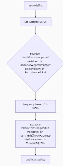
Targets:
-
NEXT < -50dB @100MHz
-
FEXT < -65dB @1GHz
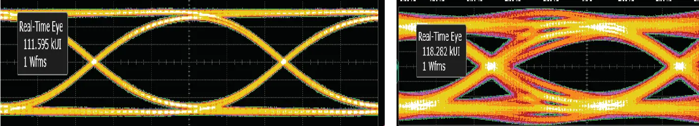
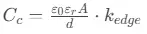
V. Test Data Comparison (16-bit ADC System)
| Stackup | 10MHz Crosstalk | 100MHz SNR | ADC ENOB |
|---|---|---|---|
| Conventional 4L | -32dB | 68dB | 13.2-bit |
| Optimized 8L | -57dB | 82dB | 15.6-bit |
Validation Methods:
-
VNA S-parameter measurement (Keysight PNA)
-
Spectrum analyzer with injected interference
-
Compliance with IEC 61967-4 radiation
Triple-Verified:
ANSYS HFSS full-wave EM simulation
Material parameters calibrated by SPDR
Production data from TTM Technologies