 PCB
PCB FPC
FPC Rigid-Flex
 FR-4
FR-4 HDI PCB
 Rogers High-Frequency Board
 PTFE Teflon High-Frequency Board
 Aluminum
 Copper Core
 PCB Assembly
 LED light PCBA
 Memory PCBA
 Power Supply PCBA
 New Energey PCBA
 Communication PCBA
 Industrial Control PCBA
 Medical Equipment PCBA
 Testing Service
 PCBA Testing Service
 Certification Application
 RoHS Certification Application
 REACH Certification Application
 CE Certification Application
 FCC Certification Application
 CQC Certification Application
 UL Certification Application
 Transformers, Inductors
 High Frequency Transformers
 Low Frequency Transformers
 High Power Transformers
 Conversion Transformers
 Sealed Transformers
 Ring Transformers
 Inductors
 Wires,Cables Customized
 Network Cables
 Power Cords
 Antenna Cables
 Coaxial Cables
 Net Position Indicator
 Solar AIS net position indicator
 Capacitors
 Connectors
 Diodes
 Embedded Processors & Controllers
 Digital Signal Processors (DSP/DSC)
 Microcontrollers (MCU/MPU/SOC)
 Programmable Logic Device(CPLD/FPGA)
 Communication Modules/IoT
 Resistors
 Through Hole Resistors
 Resistor Networks, Arrays
 Potentiometers,Variable Resistors
 Aluminum Case,Porcelain Tube Resistance
 Current Sense Resistors,Shunt Resistors
 Switches
 Transistors
 Power Modules
 Isolated Power Modules
 AC-DC Power Modules
 DC-AC Module(Inverter)
 RF and Wireless
Prevention Measures for Tombstoning Defects in 0603 and Larger SMT Components
2025-12-01
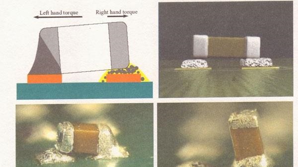
Tombstoning—also known as “drawbridging” or “standing”—is a common and costly SMT assembly defect where a chip component (e.g., Resistor, capacitor) lifts one end off the PCB pad while the other remains soldered, forming a vertical or tilted “tombstone” shape. For 0603 (1.6mm×0.8mm) and larger components, this defect not only causes electrical open circuits but also risks mechanical damage during subsequent assembly steps (e.g., conformal coating, connector insertion). Tombstoning stems from unbalanced solder paste melting and wetting forces on the two component pads, driven by factors like pad design, paste printing, component placement, and reflow profiling. This article systematically analyzes the root causes of tombstoning in 0603+ components and outlines actionable prevention measures, aligned with IPC-A-610 and IPC-7351 standards, to reduce defect rates to <0.1%.
1. Fundamentals of Tombstoning in 0603+ SMT Components
Before diving into prevention, it is critical to understand the physics and root causes of tombstoning:
1.1 Mechanism of Tombstoning
Tombstoning occurs during the reflow soldering stage when the suRFace tension of molten solder paste exerts uneven upward forces on the component’s two ends. The key sequence is:
- Solder paste melting: As the PCB enters the reflow oven’s peak zone (217–225°C for SnPb; 245–255°C for SAC305), solder paste on the component’s two pads melts at slightly different times.
- Unbalanced wetting: If one pad’s solder melts earlier or wets faster, its surface tension pulls the component toward that pad, lifting the other end off the opposite pad.
- Solidification: The molten solder solidifies with the component in a tilted/vertical position, forming a tombstone.
For 0603+ components, their larger mass (compared to 0402 or 0201) means greater momentum during solder wetting—unbalanced forces are more likely to cause severe tombstoning rather than minor tilting.
1.2 Key Risk Factors for 0603+ Components
While tombstoning affects all chip components, 0603+ parts face unique risks due to their size:
- Larger pad area: 0603 components require larger pads (per IPC-7351, typically 1.2mm×0.8mm per pad), increasing the potential for solder paste volume variation.
- Higher mass: Greater component weight requires more balanced wetting forces to keep it seated; even small solder volume differences can create enough torque to lift one end.
- Lead-frame design: Some 0603+ capacitors use asymmetric lead frames, making them more susceptible to uneven wetting if pad design does not compensate.
2. Pad Design Optimization: The Foundation of Tombstoning Prevention
PCB pad design is the first line of defense against tombstoning, as it directly controls solder paste volume, wetting area, and heat distribution. For 0603+ components, adhere to these IPC-7351-aligned guidelines:
2.1 Symmetric Pad Sizing and Placement
- Pad dimension symmetry: Ensure both pads for a component have identical length, width, and shape. For 0603 resistors/capacitors:
- Standard pad size: 1.2mm (length) × 0.8mm (width) per pad.
- Pad spacing: 0.4mm (distance between the inner edges of the two pads) to match the component’s end-to-end length (1.6mm).
- Avoid “stretched” or “shrunken” pads—even a 0.1mm difference in pad length can cause 20% variation in solder paste volume, leading to tombstoning.
- Fiducial alignment: Place local fiducials (1.0mm×1.0mm) within 2mm of the component to ensure accurate placement of both pads during PCB manufacturing. Misaligned pads (>0.05mm offset) create uneven wetting zones.
2.2 Pad Shape and Thermal Relief
- Optimal pad shape: Use rectangular pads with rounded corners (radius 0.1mm) instead of square or oval pads. Rounded corners prevent solder paste accumulation at the edges, ensuring uniform melting.
- Thermal relief for large copper areas: If the component pads are connected to large copper planes (e.g., ground or power planes), add thermal relief traces (0.2mm wide) to each pad. Large copper planes act as heat sinks, causing uneven heating of the two pads—one pad melts solder faster than the other, triggering tombstoning. Thermal relief balances heat transfer, ensuring both pads reach melting temperature simultaneously.
2.3 Solder Mask Design
- Solder mask opening symmetry: The solder mask opening (SMO) for each pad must match the pad size exactly (no overlap or undercut). For 0603 pads, SMO should be 1.3mm×0.9mm (0.05mm larger than the pad on all sides) to ensure full pad exposure.
- Avoid solder mask between pads: Do not place solder mask between the two component pads, as it can trap air or prevent solder paste from spreading evenly during reflow.
3. Solder Paste Printing Control: Ensuring Uniform Volume and Deposit
Inconsistent solder paste volume on the two component pads is the leading cause of tombstoning. For 0603+ components, precise printing control is critical:
3.1 Stencil Design for Balanced Paste Deposit
- Stencil aperture symmetry: The stencil aperture for each pad must mirror the pad size and shape. For 0603 pads (1.2mm×0.8mm), use apertures of 1.1mm×0.7mm (90% of pad size) to prevent paste bridging while ensuring sufficient volume.
- Aperture wall smoothness: Use laser-cut or electroformed stencils with smooth inner walls (Ra <0.8μm). Rough walls cause uneven paste release, leading to volume variations of >15% between the two pads.
- Stencil thickness: For 0603+ components, use a 0.12mm thick stencil (instead of 0.1mm) to increase solder paste volume (target: 0.08–0.10mm³ per pad). Insufficient paste volume (<0.06mm³) reduces wetting force, making the component prone to lifting.
3.2 Printing Process Optimization
- Squeegee pressure and speed: Use a stainless-steel squeegee with a 60° angle, applying 20–30N pressure at 20–30mm/s speed. Too much pressure (>35N) squeezes excess paste from one pad; too little pressure (<15N) leaves insufficient paste.
- Print gap: Maintain a 0.1mm print gap between the stencil and PCB. A larger gap causes paste “bleeding” (volume increase) on one side; a smaller gap leads to uneven paste transfer.
- Paste release: Use a stencil with a 5–10μm nano-coating to improve paste release. After printing, inspect paste deposits with SPI (Solder Paste Inspection) to ensure volume variation between the two pads is <5%. Reject PCBs with volume differences >8%.
4. Component Placement Precision: Minimizing Offset and Tilt
Even with optimal pad and stencil design, poor component placement can introduce tombstoning risks. For 0603+ components, focus on these placement parameters:
4.1 Centering and Offset Control
- X/Y offset: Ensure the component is centered over the two pads with X/Y offset <0.05mm. An offset of >0.1mm means one end of the component sits on more solder paste than the other, creating unbalanced wetting forces.
- Rotation offset: Limit rotation offset to <2°. Rotated components (>3°) have one end overlapping the pad edge, reducing wetting area and increasing lift risk.
- Placement pressure: Use 50–100g placement pressure. Too much pressure (>150g) squeezes solder paste out from under one end; too little pressure (<30g) leaves the component loosely seated, allowing solder tension to lift it.
4.2 Component Handling and Orientation
- Anti-static packaging: Store 0603+ components in anti-static tubes or trays to prevent electrostatic discharge (ESD) damage, which can deform lead frames and cause asymmetric seating.
- Orientation consistency: For polarized components (e.g., tantalum capacitors), ensure correct polarity during placement. Reversed polarity does not directly cause tombstoning but can lead to component failure, which may be misdiagnosed as tombstoning.
5. Reflow Profiling: Balancing Heating and Wetting
Reflow oven temperature profiling is critical for ensuring both solder pads melt simultaneously and wet evenly. For 0603+ components, optimize the reflow profile as follows:
5.1 Preheat Zone: Uniform Temperature Ramp
- Ramp rate: Maintain a preheat ramp rate of 1–2°C/sec (from 25°C to 150°C). A fast ramp rate (>3°C/sec) causes uneven heating—one pad reaches melting temperature before the other. A slow ramp rate (<0.5°C/sec) leads to excessive flux evaporation, reducing solder wetting.
- Preheat hold time: Hold at 150–170°C for 60–90 seconds. This ensures the entire PCB (including pads and components) reaches a uniform temperature before the soak zone.
5.2 Soak Zone: Flux Activation and Oxide Removal
- Soak temperature: Maintain 170–190°C for 40–60 seconds. This activates the flux, which removes oxide layers from the component leads and PCB pads. Insufficient soak time (<30 seconds) leaves oxides intact, reducing wetting; excessive soak time (>70 seconds) burns flux, creating a residue that inhibits wetting.
5.3 Reflow Zone: Controlled Peak Temperature and Time
- Peak temperature: Set peak temperature to 220–225°C for SnPb solder or 245–250°C for SAC305 lead-free solder. The component’s two pads must reach peak temperature within ±1°C of each other to ensure simultaneous solder melting.
- Time above liquidus (TAL): Maintain TAL at 40–60 seconds. Too short TAL (<30 seconds) means solder does not fully wet; too long TAL (>70 seconds) causes solder balling and pad oxidation.
- Cooling rate: Use a cooling ramp rate of 2–3°C/sec (from peak temperature to 150°C). Fast cooling (>4°C/sec) causes solder to solidify before the component settles; slow cooling (<1°C/sec) allows excessive solder movement, increasing tombstoning risk.
6. Material and Environmental Control: Reducing External Variables
External factors like component quality, solder paste properties, and environmental conditions can contribute to tombstoning. Implement these controls:
6.1 Component Quality Assurance
- Lead frame inspection: Verify 0603+ components have flat, clean lead frames with no oxidation (Ra <1.0μm). Oxidized leads (>0.5μm oxide layer) reduce wetting, leading to uneven solder tension.
- Dimensional consistency: Ensure component length, width, and thickness variation is <0.05mm. Components with out-of-spec dimensions (e.g., one end thicker than the other) sit unevenly on the pads.
6.2 Solder Paste Management
- Storage and handling: Store solder paste at 2–10°C and thaw at room temperature for 4–6 hours before use. Do not refreeze thawed paste, as it separates and loses consistency.
- Mixing: Stir paste manually for 2 minutes or use a paste mixer for 60 seconds to ensure homogeneity. Unmixed paste has uneven particle distribution, leading to inconsistent melting.
- Pot life: Use solder paste within 8 hours of opening. Paste left exposed to air (>12 hours) absorbs moisture and oxidizes, reducing wetting performance.
6.3 Environmental Control
- Temperature and humidity: Maintain the SMT line environment at 20–25°C and 40–60% RH. High humidity (>65% RH) causes solder paste to absorb moisture, leading to spattering during reflow; low humidity (<30% RH) increases static buildup, damaging components.
7. Inspection, Testing, and Continuous Improvement
Preventive measures must be validated with robust inspection and continuous monitoring:
7.1 In-Line Inspection
- SPI inspection: After printing, use SPI to check solder paste volume, height, and area on both pads. Reject PCBs with volume variation >5% or height variation >10%.
- AOI inspection: After placement, use AOI to verify component offset, rotation, and seating. Reject PCBs with offset >0.05mm or rotation >2°.
- X-ray inspection: After reflow, use X-ray to inspect solder joints for tombstoning, bridging, or voids. For 0603+ components, X-ray can detect even subtle tilting (>5°) that may not be visible to the naked eye.
7.2 Root Cause Analysis (RCA)
When tombstoning occurs, use the 5-Why method to identify the root cause:
- Why did the component tombstone? Unbalanced solder wetting.
- Why was wetting unbalanced? Solder paste volume on Pad A was 15% higher than Pad B.
- Why was volume unbalanced? Stencil aperture for Pad A was 0.1mm wider than Pad B.
- Why was the aperture mis-sized? Stencil design did not match the latest PCB pad layout.
- Why was the design not updated? No formal review process for stencil-PCB alignment.
Implement corrective actions (e.g., updating stencil design, adding a review process) to prevent recurrence.
7.3 Continuous Process Improvement
- Data collection: Track tombstoning rates by component type, production shift, and machine. Use statistical process control (SPC) to identify trends (e.g., higher defects during the third shift due to temperature fluctuations).
- Regular audits: Conduct monthly audits of pad designs, stencil quality, and reflow profiles to ensure compliance with standards.
- Operator training: Train SMT operators to recognize tombstoning risks (e.g., uneven paste, component offset) and take corrective action immediately.
8. Conclusion
Tombstoning in 0603 and larger SMT components is a preventable defect rooted in unbalanced solder wetting forces. By implementing a holistic approach—optimizing pad design for symmetry and thermal balance, controlling solder paste printing for uniform volume, ensuring precise component placement, optimizing reflow profiling for simultaneous melting, and managing materials/environments—manufacturers can reduce tombstoning rates to <0.1%. Critical to success is rigorous in-line inspection (SPI, AOI, X-ray) and continuous improvement through data analysis and process audits. Adhering to these measures not only improves production yield but also ensures the reliability of PCB assemblies in applications ranging from consumer electronics to automotive systems, where even a single tombstone can cause costly field failures.