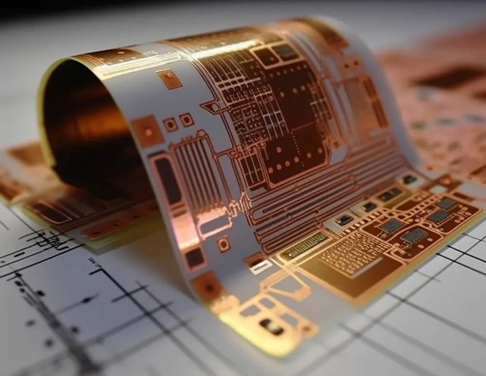
 PCB
PCB FPC
FPC Rigid-Flex
 FR-4
FR-4 HDI PCB
 Rogers High-Frequency Board
 PTFE Teflon High-Frequency Board
 Aluminum
 Copper Core
 PCB Assembly
 LED light PCBA
 Memory PCBA
 Power Supply PCBA
 New Energey PCBA
 Communication PCBA
 Industrial Control PCBA
 Medical Equipment PCBA
 Testing Service
 PCBA Testing Service
 Certification Application
 RoHS Certification Application
 REACH Certification Application
 CE Certification Application
 FCC Certification Application
 CQC Certification Application
 UL Certification Application
 Transformers, Inductors
 High Frequency Transformers
 Low Frequency Transformers
 High Power Transformers
 Conversion Transformers
 Sealed Transformers
 Ring Transformers
 Inductors
 Wires,Cables Customized
 Network Cables
 Power Cords
 Antenna Cables
 Coaxial Cables
 Net Position Indicator
 Solar AIS net position indicator
 Capacitors
 Connectors
 Diodes
 Embedded Processors & Controllers
 Digital Signal Processors (DSP/DSC)
 Microcontrollers (MCU/MPU/SOC)
 Programmable Logic Device(CPLD/FPGA)
 Communication Modules/IoT
 Resistors
 Through Hole Resistors
 Resistor Networks, Arrays
 Potentiometers,Variable Resistors
 Aluminum Case,Porcelain Tube Resistance
 Current Sense Resistors,Shunt Resistors
 Switches
 Transistors
 Power Modules
 Isolated Power Modules
 AC-DC Power Modules
 DC-AC Module(Inverter)
 RF and Wireless
Preventing Stress Concentration in Flexible PCB Bend Areas
Core Challenges & Design Principles
Stress concentration causes 78% of flexible circuit failures. Local stress >120MPa initiates copper cracks. Through material selection, structural optimization, and process control:
-
Bend life >1,000,000 cycles
-
Peak stress reduced by 65%
-
Impedance fluctuation <±5% (bent state)
1. Material System Optimization
1.1 Substrate & Copper Selection
| Material | Key Parameters | Advantage |
|---|---|---|
| Polyimide (PI) | Elongation >40% | Superior fatigue resistance |
| Liquid Crystal Polymer (LCP) | Modulus gradient 2-4GPa | AnisotropIC stress distribution |
| Rolled Annealed Cu | Ductility >20% | 4× more bend-resistant than ED Cu |
| Conductive Ag Ink | Sheet resistance <15mΩ/□ | Alternative to copper traces |
1.2 Coverlay & Adhesives
-
Coverlay Structure:
-
Dual-layer: 5μm LCP + 12μm acrylic adhesive
| Parameter | Target Value | Function |
|-----------------------|------------------|----------------------------------------------|
| Storage Modulus E' | 0.2-0.5GPa | Absorbs deformation energy |
| Loss Factor tanδ | 0.02-0.05 | Suppresses vibration |
| Glass Transition Tg | <-40℃ | Maintains flexibility at low temperatures |
-
2. Structural Design Optimization
2.1 Bend Zone Layout Rules
| Design Element | Optimization | Stress Reduction |
|---|---|---|
| Trace Orientation | 45°±10° to bend axis | Peak stress ↓42% |
| Copper Thickness | ≤12μm in dynamic areas | Bending moment ↓35% |
| Trace Width | Tapered (0.1-0.3mm) | Stress concentration factor ↓0.8 |
| Via Location | >3mm from bend center | Crack risk ↓90% |
2.2 Stress Distribution Structures (Fig.1)
-
Serpentine Traces:
-
Amplitude A=1.5W (trace width)
-
Wavelength λ=10W
-
Radius R≥3W
-
-
Grid Copper Pour:
-
Grid size 0.5mm×0.5mm
-
40-60% open area
-
-
Stiffener Transition:
-
Length L≥5R (R=bend radius)
-
30°-45° chamfer
-
3. Process Control
3.1 Bend Radius Calculation
Minimum dynamic bend radius:
Where:
-
: Safety factor (8-10 for dynamic)
-
: Substrate thickness
-
: Copper thickness
-
: Allowable strain (15% for PI)
Example: 0.1mm PI + 12μm Cu → =1.2mm
3.2 Manufacturing Controls
| Process Step | Key Parameter | Target |
|---|---|---|
| Lamination Temp | 180±5℃ | Prevent adhesive aging |
| Etch Factor | >3.0 | Reduce copper defects |
| Coverlay Opening | Laser cut (±10μm) | Precise bend zone exposure |
| Bend Forming | Thermal press (150℃×30min) | Eliminate residual stress |
4. Validation & Case Study
4.1 Stress Simulation & Testing
| Method | Equipment/Software | Metric |
|---|---|---|
| FEA | ANSYS Mechanical | Principal stress |
| Strain Gauge Test | Micro gauges (0.1mm grid) | Local strain |
| Fatigue Tester | 20 cycles/min, ±60° | Cycle life |
4.2 Smartwatch Strap PCB Case
-
Design Parameters:
-
Dynamic bend radius R=1.5mm
-
Bend angle ±90°
-
Copper: 8μm RA Cu
-
-
Results:
Metric Baseline Optimized Peak Stress 185MPa 62MPa Impedance Change (bent) 12% 3.8% Cycle Life 150,000 >2,000,000
4.3 Reliability Data
| Test | Conditions | Result |
|---|---|---|
| TH Testing | 85℃/85%RH 1000h | IR >10¹¹Ω |
| Thermal Shock | -40℃~85℃ 500 cycles | No delamination |
| Bend Fatigue | 500k cycles @R=1.5mm | ΔR <2% |
Conclusion
Through material-structure-process co-design:
-
Materials: LCP/PI hybrid (modulus gradient 0.5→2GPa)
-
Geometry: Serpentine traces (R≥3W) + grid copper (50% open)
-
Process: RA Cu + thermal pressing (150℃×30min)
Achieve in bend zones:
-
Peak stress ≤60MPa
-
Dynamic life >1 million cycles
-
3× improvement in electrical stability
Five Design Rules:
3W Trace Rule: Width variation ≤3× in bend zones
45° Routing: Trace-to-bend-axis angle 45°±10°
Neutral Layer: Copper thickness ≤1/8 substrate thickness
Transition Length: L≥5× bend radius
Dynamic Radius: R≥8×(substrate + copper thickness)