 PCB
PCB FPC
FPC Rigid-Flex
 FR-4
FR-4 HDI PCB
 Rogers High-Frequency Board
 PTFE Teflon High-Frequency Board
 Aluminum
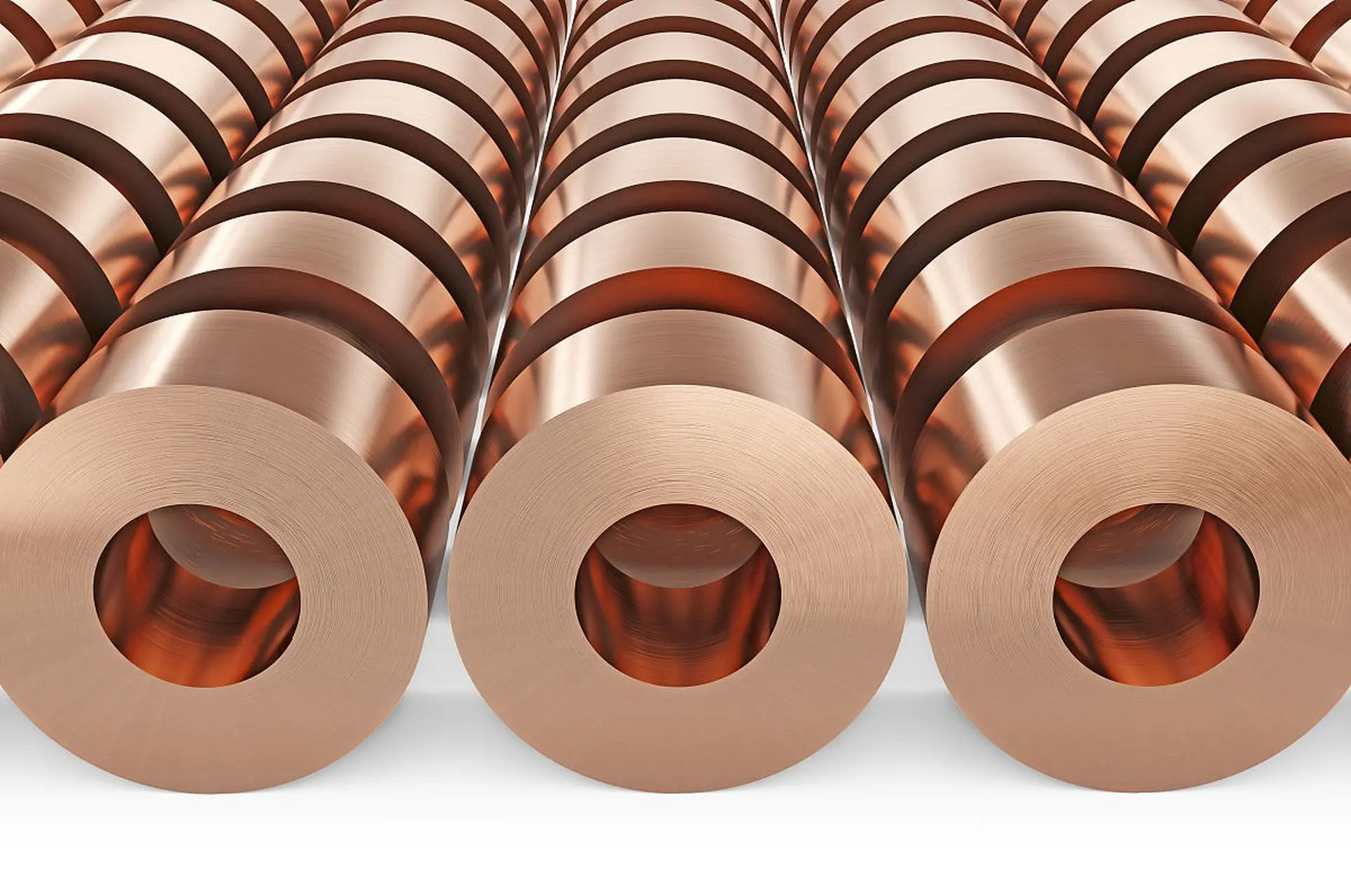
 Copper Core
 PCB Assembly
 LED light PCBA
 Memory PCBA
 Power Supply PCBA
 New Energey PCBA
 Communication PCBA
 Industrial Control PCBA
 Medical Equipment PCBA
 Testing Service
 PCBA Testing Service
 Certification Application
 RoHS Certification Application
 REACH Certification Application
 CE Certification Application
 FCC Certification Application
 CQC Certification Application
 UL Certification Application
 Transformers, Inductors
 High Frequency Transformers
 Low Frequency Transformers
 High Power Transformers
 Conversion Transformers
 Sealed Transformers
 Ring Transformers
 Inductors
 Wires,Cables Customized
 Network Cables
 Power Cords
 Antenna Cables
 Coaxial Cables
 Net Position Indicator
 Solar AIS net position indicator
 Capacitors
 Connectors
 Diodes
 Embedded Processors & Controllers
 Digital Signal Processors (DSP/DSC)
 Microcontrollers (MCU/MPU/SOC)
 Programmable Logic Device(CPLD/FPGA)
 Communication Modules/IoT
 Resistors
 Through Hole Resistors
 Resistor Networks, Arrays
 Potentiometers,Variable Resistors
 Aluminum Case,Porcelain Tube Resistance
 Current Sense Resistors,Shunt Resistors
 Switches
 Transistors
 Power Modules
 Isolated Power Modules
 AC-DC Power Modules
 DC-AC Module(Inverter)
 RF and Wireless
Preventing Sidewall Serration in Low-Profile Copper (HVLP) Etching
Hyper Very Low Profile (HVLP) copper foil (Rz<3μm) is critICal for high-frequency PCBs, where etching quality directly impacts signal integrity. Sidewall serration—periodic edge roughness (>0.5μm)—causes additional 0.2dB/cm loss at mmWave frequencies.
1. Serration Formation Mechanisms
1.1 Micro-Etching Dynamics (Figure 1)
Copper etching anisotropy:
Cu+2FeCl3→CuCl2+2FeCl2
Serration arises from competing processes:
-
Vertical etching: Grain boundary preferential dissolution;
-
Lateral undercut: Chemical seepage at resist edges.
1.2 Critical Factors
-
Resist slope angle: <70° increases undercut risk by 30%;
-
SuRFace tension: >40mN/m causes non-uniform wetting;
-
Crystal orientation: <100> etches 1.8x faster than <111>.
2. Etchant Formulation Optimization
2.1 Advanced Chemistry
| Component | Concentration | Function |
|---|---|---|
| FeCl₃ | 2.0-2.5mol/L | Main oxidizer |
| H₂SO₄ | 0.5-1.0mol/L | Stabilizes Fe³+ |
| PEG-600 | 0.3-0.5g/L | Reduces surface tension |
| Benzoimidazole (BIA) | 0.1-0.2g/L | Grain boundary inhibitor |
| Alkyl sulfonate | 0.05-0.1g/L | Wetting agent |
2.2 Parameter Monitoring
-
Specific gravity: 1.32±0.02g/cm³ (refractometry);
-
ORP: 450-500mV (vs. Ag/AgCl);
-
Fe²+: <0.15mol/L (electrolytic regeneration if exceeded).
3. Process Parameter Tuning
3.1 Spray & Transport
-
Pressure: 0.8-1.2bar (high pressure damages resist);
-
Nozzle angle: 15° tilt for laminar flow (turbulence <5%);
-
Speed: 1.2-1.5m/min (etch factor 2.5-3.0).
3.2 Temperature & Time
-
Temperature: 50±1℃ (>2℃ fluctuation triggers orientation-selective etching);
-
Multi-stage etching:
-
Pre-etch: 30s for oxide removal;
-
Main etch: 90s for vertical profile;
-
Finishing: 20s with PEG for sidewall smoothing.
-
4. Equipment Engineering
4.1 Spray Chamber Design
-
Zoned flow: Independent upper/lower nozzles to compensate gravity effects;
-
Vortex suppressor: Honeycomb baffles reduce Reynolds number <2000.
4.2 Resist Lamination
-
Vacuum chuck: Porous ceramic (10μm pores), -60kPa pressure;
-
Pre-bake: 75℃×5min to eliminate resist-copper gaps (<0.1μm).
5. Defect Inspection & Validation
5.1 Sidewall Characterization
-
Laser confocal microscopy: 3D profile analysis of serration period/amplitude (Figure 2);
-
SEM: Grain boundary inspection to evaluate BIA performance.
5.2 Electrical Testing
-
Impedance consistency: ±1.5% intra-board variation (10GHz);
-
Insertion loss: 0.18dB/cm reduction at 28GHz.
6. Case Studies & Data
6.1 77GHz Automotive Radar
-
Copper: HVLP Rz=2.1μm;
-
Parameters:
-
Etchant: FeCl₃ 2.3mol/L + PEG-600 0.4g/L;
-
Spray: 1.0bar, 52℃;
-
-
Results:
Metric Before After Serration (μm) 0.72 0.15 Impedance error ±3.8% ±1.2% Etch factor 1.8 3.1
6.2 Reliability Tests
-
Thermal shock: -40℃~125℃, 500 cycles (no micro-cracks);
-
Humidity aging: 85℃/85%RH, 1000h (<0.5% impedance drift).