 PCB
PCB FPC
FPC Rigid-Flex
 FR-4
FR-4 HDI PCB
 Rogers High-Frequency Board
 PTFE Teflon High-Frequency Board
 Aluminum
 Copper Core
 PCB Assembly
 LED light PCBA
 Memory PCBA
 Power Supply PCBA
 New Energey PCBA
 Communication PCBA
 Industrial Control PCBA
 Medical Equipment PCBA
 Testing Service
 PCBA Testing Service
 Certification Application
 RoHS Certification Application
 REACH Certification Application
 CE Certification Application
 FCC Certification Application
 CQC Certification Application
 UL Certification Application
 Transformers, Inductors
 High Frequency Transformers
 Low Frequency Transformers
 High Power Transformers
 Conversion Transformers
 Sealed Transformers
 Ring Transformers
 Inductors
 Wires,Cables Customized
 Network Cables
 Power Cords
 Antenna Cables
 Coaxial Cables
 Net Position Indicator
 Solar AIS net position indicator
 Capacitors
 Connectors
 Diodes
 Embedded Processors & Controllers
 Digital Signal Processors (DSP/DSC)
 Microcontrollers (MCU/MPU/SOC)
 Programmable Logic Device(CPLD/FPGA)
 Communication Modules/IoT
 Resistors
 Through Hole Resistors
 Resistor Networks, Arrays
 Potentiometers,Variable Resistors
 Aluminum Case,Porcelain Tube Resistance
 Current Sense Resistors,Shunt Resistors
 Switches
 Transistors
 Power Modules
 Isolated Power Modules
 AC-DC Power Modules
 DC-AC Module(Inverter)
 RF and Wireless
Packaging Scheme Improvements to Prevent Component Loosening or Falling Off PCBA During Transportation Vibration
2025-12-27
Printed Circuit Board Assemblies (PCBAs) are core components of electronic products, integrating a variety of suRFace mount devices (SMDs) such as BGAs, QFPs, chip resistors, and capacitors, as well as through-hole components. During transportation, PCBAs are inevitably subjected to vibration impacts from vehicles, logistics handling, and stacking operations. These vibrations, if exceeding the component’s tolerance threshold, can cause solder joint fatigue, component loosening, or even complete detachment—defects that directly lead to product functional failures, increased rework costs, and reduced customer trust.
The root cause of component loosening or falling off due to transportation vibration lies in the mismatch between the packaging system’s vibration isolation capability and the PCBA’s structural vulnerability. Traditional packaging schemes (e.g., simple bubble wrap + carton) often fail to effectively attenuate low-frequency vibrations (5-50 Hz) that are most destructive to solder joints. This article provides a comprehensive analysis of packaging scheme improvements to mitigate such risks, covering vibration damage mechanisms, component-specific vulnerability analysis, buffer material selection, structural design optimization, and validation testing. References to industry standards such as IEC 60068-2-6 (Vibration Testing) and ASTM D4169 (Standard Practice for Performance Testing of Shipping Containers and Systems) are integrated to ensure the proposed improvements are compliant and practical. Case studies of successful packaging upgrades are also included to illustrate the application of these strategies.
1. Vibration Damage Mechanisms to PCBA Components During Transportation
Transportation vibration is a complex multi-frequency excitation, typically ranging from 1 Hz (low-frequency jostling) to 2000 Hz (high-frequency resonance). The damage to PCBA components is mainly caused by three interrelated mechanisms: solder joint fatigue, component resonance, and structural stress concentration. Understanding these mechanisms is the foundation for designing effective packaging improvements.
1.1 Solder Joint Fatigue Failure
Solder joints (e.g., Sn-Ag-Cu lead-free solder joints) are the critical connections between components and PCB pads. Under cyclic vibration, solder joints undergo repeated elastic-plastic deformation, leading to fatigue crack initiation and propagation. This process is accelerated by: Low-Frequency Vibration (5-50 Hz): Dominant in road and sea transportation, this frequency range matches the natural frequency of most PCBAs (10-30 Hz), causing amplified displacement and severe solder joint stress. High Acceleration Amplitude: Vibration acceleration (measured in g-force) during truck transportation can reach 1-3 g, while rough handling (e.g., dropping) may exceed 10 g, leading to instantaneous solder joint failure. Solder Joint Geometry: Smaller solder joints (e.g., 01005 chip components) or fine-pitch joints (e.g., 0.4 mm pitch QFPs) have lower fatigue resistance due to their reduced cross-sectional area.
Fatigue failure typically starts at the solder joint-pad interface and progresses inward, eventually causing component loosening or electrical disconnection. For BGAs, this often manifests as "ball shear" or "ball pull" failures, where solder balls detach from either the BGA package or the PCB pad.
1.2 Component Resonance Damage
Each electronic component has a unique natural frequency, determined by its mass, stiffness, and attachment method. When transportation vibration frequency matches the component’s natural frequency, resonance occurs, resulting in amplified displacement (up to 10x the input vibration amplitude). This is particularly problematic for: Heavy Components: Large BGAs (≥300 balls), power Modules, or connectors have higher mass, leading to lower natural frequencies (5-20 Hz) that easily align with transportation vibration frequencies.Tall Components: Capacitors with tall cylindrical packages or connectors with extended pins have higher center-of-mass, increasing rotational inertia and resonance-induced stress on solder joints.Unsupported Components: Components with no additional mechanical fixation (relying solely on solder joints) are more prone to resonance damage.
Resonance-induced vibration can cause not only solder joint failure but also physical damage to component packages (e.g., cracked ceramic bodies in capacitors, bent connector pins).
1.3 Structural Stress Concentration
The PCB itself acts as a structural substrate for components. During vibration, the PCB bends and flexes, creating stress concentrations at component attachment points—especially at the edges of the PCB or near large cutouts. This stress is transferred to the solder joints, accelerating fatigue. Factors that exacerbate structural stress include: PCB Thickness: Thin PCBs (≤0.8 mm) have lower bending stiffness, leading to greater flexure under vibration.Component Placement: Components placed near PCB edges or corners experience higher stress due to the PCB’s larger deflection in these areas.Uneven Component Distribution: Concentrated placement of heavy components on one side of the PCB creates unbalanced mass distribution, increasing bending stress during vibration.
2. Vulnerability Analysis of Different PCBA Components to Vibration
Not all components are equally susceptible to vibration-induced loosening or falling off. Understanding the vulnerability of different component types helps prioritize packaging improvements. Below is a detailed analysis of key component categories:
2.1 Surface Mount Devices (SMDs)
2.1.1 Ball Grid Arrays (BGAs)
BGAs are highly vulnerable due to their large mass, fine-pitch solder balls, and reliance on multiple small solder joints for attachment. Large BGAs (e.g., 40x40 mm with 400+ balls) have a natural frequency of 8-15 Hz, which overlaps with typical transportation vibration frequencies. Vibration-induced shear stress on individual solder balls can lead to partial or complete ball detachment. Additionally, BGA packages with low coefficient of thermal expansion (CTE) mismatch with the PCB are more prone to solder joint fatigue under vibration.
2.1.2 Quad Flat Packages (QFPs)
QFPs with fine pitches (≤0.5 mm) have delicate lead-solder joint connections. Vibration causes the leads to bend slightly, creating cyclic stress at the lead-solder interface. This leads to fatigue cracks in the solder joints, especially for QFPs with a large number of leads (≥200), where the cumulative stress from multiple leads exacerbates damage. The leads themselves may also bend or break if vibration amplitude is excessive.
2.1.3 Chip Components (Resistors/Capacitors)
Small chip components (01005, 0201) have minimal mass but rely on tiny solder joints (≤0.5 mm²) for attachment. While their natural frequency is high (50-100 Hz), high-frequency vibration (e.g., from air transportation or mechanical handling) can cause solder joint fatigue. Larger chip components (0603, 0805) are more vulnerable due to their higher mass, with a higher risk of solder joint failure under low-frequency vibration.
2.2 Through-Hole Components (THCs)
THCs (e.g., connectors, electrolytic capacitors) are generally more vibration-resistant than SMDs due to their mechanical insertion into PCB holes and solder fillet formation on both sides of the PCB. However, large or heavy THCs (e.g., power connectors, transformers) can still loosen or fall off if subjected to high acceleration vibration. The solder fillets of THCs are prone to cracking under cyclic bending stress, especially if the component is not mechanically secured.
2.3 Special Components
Components such as sensors, LEDs, and oscillators are often more vibration-sensitive due to their delicate internal structures. For example, MEMS sensors have tiny moving parts that can be damaged by excessive vibration, while LED packages with thin leads are prone to solder joint failure. These components require additional packaging protection beyond standard measures.
3. Key Principles for Packaging Scheme Improvement
The goal of packaging improvement is to design a system that effectively isolates PCBA from destructive transportation vibrations, reduces stress on components and solder joints, and maintains structural stability. The key principles guiding packaging improvements are:
3.1 Vibration Isolation
Vibration isolation is the primary strategy to reduce vibration transmission from the external environment to the PCBA. The packaging system should attenuate vibration amplitudes in the critical frequency range (5-50 Hz) by at least 80%. This is achieved through the use of buffer materials with appropriate stiffness and damping properties, which absorb and dissipate vibration energy.
3.2 Load Distribution and Fixation
Uniform load distribution prevents localized stress concentration on the PCBA. The packaging should securely fix the PCBA (or its enclosure) to minimize relative movement, while avoiding over-constraint that could introduce additional stress. For heavy components, additional mechanical fixation (e.g., foam inserts, straps) should be used to reduce stress on solder joints.
3.3 Environmental Protection
While vibration is the primary concern, the packaging should also protect against moisture, dust, and temperature fluctuations—factors that can weaken solder joints and exacerbate vibration damage. For example, moisture absorption can reduce solder joint strength, making components more prone to falling off under vibration.
3.4 Compatibility with Logistics Operations
Improved packaging should not compromise logistics efficiency. It should be lightweight, stackable, and easy to handle, while maintaining sufficient durability to withstand stacking pressure and rough handling. The packaging should also be cost-effective, especially for high-volume production.
4. Detailed Packaging Improvement Strategies
Based on the above principles, the following improvements can be implemented to prevent component loosening or falling off during transportation:
4.1 Buffer Material Selection and Optimization
Buffer materials are the core of vibration isolation. The selection of buffer materials should be based on the PCBA’s weight, vibration tolerance, and transportation environment. Common buffer materials and their applications are as follows:
4.1.1 Polyethylene Foam (PE Foam)
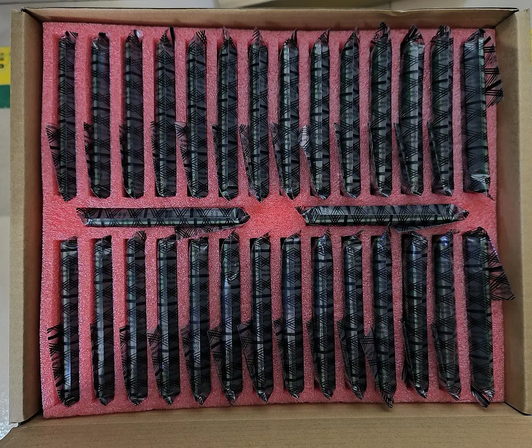
PE foam is a cost-effective buffer material with good damping properties and resilience. It is suitable for lightweight PCBAs (≤500 g) and low-to-moderate vibration environments. Key improvements include: Density Selection: Use high-density PE foam (40-60 kg/m³) for better load-bearing capacity and vibration isolation. Low-density foam (≤30 kg/m³) is too soft and may not provide sufficient support for heavy components.Thickness Optimization: The foam thickness should be at least 20 mm to effectively attenuate low-frequency vibration. For high-vibration environments (e.g., road transportation), increase thickness to 30-50 mm.Custom Cutting: Use CNC-cut PE foam inserts with precision cavities that match the PCBA’s shape. This ensures tight fit and uniform support, reducing relative movement.
4.1.2 Polyurethane Foam (PU Foam)
PU foam has superior damping properties compared to PE foam, making it suitable for heavy PCBAs (≥500 g) or high-vibration environments. It is available in various hardness levels (Shore A 20-80), allowing customization for specific PCBA requirements. Key applications: Soft PU Foam (Shore A 20-30): Used for delicate components (e.g., MEMS sensors, LEDs) to provide gentle support and vibration absorption.Medium-Hard PU Foam (Shore A 40-60): Ideal for general-purpose PCBA packaging, balancing support and vibration isolation.Hard PU Foam (Shore A 70-80): Used for heavy components (e.g., power modules, transformers) to provide rigid support and prevent excessive deflection.
4.1.3 Air Cushions and Bubble Wrap
Air cushions and bubble wrap are suitable for supplementary protection or lightweight PCBAs. However, they are less effective for low-frequency vibration isolation compared to foam. Improvements include: Multi-Layer Wrapping: Use 2-3 layers of bubble wrap (with 10-15 mm bubble diameter) for enhanced vibration absorption.Air Cushion Placement: Place air cushions around the PCBA’s edges and corners (high-stress areas) to provide targeted protection against impact and vibration.
4.1.4 Advanced Materials: Viscoelastic Polymers
For high-reliability applications (e.g., aerospace, medical devices), viscoelastic polymers (e.g., butyl rubber, silicone-based materials) are ideal. These materials exhibit both viscous and elastic properties, effectively dissipating vibration energy across a wide frequency range. They are often used as damping pads between the PCBA and its enclosure, reducing resonance-induced vibration.
4.2 Packaging Structure Design Optimization
The packaging structure plays a critical role in distributing vibration stress and securing the PCBA. Key structural improvements include:
4.2.1 Double-Layer Packaging Design
Adopt a double-layer packaging system (inner tray + outer carton) to enhance vibration isolation. The inner tray (made of foam or plastic) holds the PCBA securely, while the outer carton (corrugated cardboard with reinforced edges) provides mechanical protection. Key design features: Inner Tray Material: Use foam-in-place (FIP) polyurethane foam for the inner tray. FIP foam conforms to the PCBA’s shape during curing, providing custom-fit support and maximum vibration isolation.Outer Carton Reinforcement: Use double-wall corrugated cardboard (E-flute or B-flute) for the outer carton. Reinforce the bottom, top, and edges with additional cardboard layers or plastic corners to withstand stacking pressure and impact.Gap Filling: Fill any gaps between the inner tray and outer carton with foam inserts to prevent relative movement and enhance vibration absorption.
4.2.2 PCBA Fixation Methods
Secure the PCBA within the packaging to minimize relative movement. Common fixation methods include: Foam Inserts with Cavities: CNC-machined foam inserts with precise cavities that hold the PCBA snugly. The cavity should be slightly smaller (0.5-1 mm) than the PCBA to ensure a tight fit without excessive pressure.Adhesive Tapes: Use high-strength, vibration-resistant adhesive tapes (e.g., acrylic foam tapes) to attach the PCBA to the foam tray. Ensure the tape covers at least 30% of the PCBA’s bottom surface for secure fixation.Mechanical Clips or Straps: For heavy PCBAs, use plastic clips or elastic straps to secure the PCBA to the tray. Ensure the clips/straps apply uniform pressure and do not damage components.
4.2.3 Component-Specific Protection
Provide targeted protection for high-vulnerability components: Heavy Components: Add additional foam pads under large BGAs, power modules, or connectors to reduce stress on their solder joints. For transformers or large connectors, use foam blocks to brace the component and prevent movement.Fine-Pitch Components: Cover QFPs, BGAs, or other fine-pitch components with a thin layer of soft foam (Shore A 20-30) to prevent direct vibration impact. Ensure the foam does not contact component leads or balls.Edge Components: Components placed near PCB edges are more prone to stress. Add foam bumpers along the PCB edges to absorb vibration and reduce bending stress.
4.3 Environmental Protection Integration
Incorporate environmental protection features into the packaging to enhance component stability: Moisture Barrier: Use moisture-barrier bags (MBBs) with desiccants to package PCBAs, especially for lead-free solder joints that are sensitive to moisture. Include a humidity indicator (HI) to monitor moisture levels.Dust Protection: Seal the inner tray with a plastic film or lid to prevent dust contamination, which can weaken solder joints and cause electrical issues.Temperature Stabilization: For temperature-sensitive components (e.g., lithium-ion batteries, certain sensors), use insulated packaging with thermal liners to minimize temperature fluctuations during transportation.
4.4 Labeling and Handling Instructions
Proper labeling and handling instructions reduce the risk of rough handling during logistics: Vibration-Sensitive Labels: Apply "FRAGILE – VIBRATION SENSITIVE" labels on the outer carton, indicating the maximum allowable acceleration (e.g., "MAX 1 g") and transportation orientation (e.g., "KEEP FLAT").Handling Instructions: Include a document inside the carton with detailed handling instructions, such as "DO NOT DROP," "STACK MAX 3 LAYERS," and "USE PALLETS FOR TRANSPORTATION."Tracking Labels: Use barcode or RFID labels to track the package’s transportation history, allowing identification of potential high-vibration events (e.g., rough handling at a logistics hub).
5. Packaging Validation and Testing
Improved packaging schemes must be validated through standardized testing to ensure they meet vibration resistance requirements. Key tests include:
5.1 Vibration Testing (per IEC 60068-2-6)
Vibration testing evaluates the packaging’s ability to isolate vibration and protect the PCBA. Two main test methods are used: Sinusoidal Vibration Test: Applies sinusoidal vibration across a frequency range of 10-2000 Hz, with acceleration amplitudes up to 3 g. This test identifies resonance frequencies and evaluates solder joint fatigue resistance.Random Vibration Test: Applies random vibration with a frequency spectrum similar to real transportation environments (e.g., road, sea, air). The test uses a power spectral density (PSD) curve to simulate vibration energy distribution, with acceleration levels up to 5 g. This is the most realistic test for evaluating transportation vibration resistance.
After testing, the PCBA should be inspected for component loosening, solder joint cracks, or functional failures using visual inspection, X-ray imaging (for BGA/QFP solder joints), and electrical testing.
5.2 Impact Testing (per ASTM D4169)
Impact testing simulates rough handling (e.g., dropping, stacking) to evaluate the packaging’s ability to absorb impact energy. Common tests include: Drop Test: Drops the packaged PCBA from a height of 60-120 cm (depending on package weight) onto a concrete surface. The PCBA is inspected for component damage after each drop.Stacking Test: Stacks multiple packaged PCBAs (up to the maximum intended stack height) for 24 hours, then inspects for packaging deformation and PCBA damage.
5.3 Field Trial Validation
After laboratory testing, conduct field trials by shipping the improved packaging to different locations (e.g., domestic, international) using typical logistics routes. Track vibration levels during transportation using data loggers (e.g., accelerometers) and inspect the PCBAs upon arrival. This validates the packaging’s performance in real-world conditions.
6. Case Study: Packaging Upgrade for Automotive PCBA
An automotive electronics manufacturer was experiencing a 5% defect rate in PCBAs (used in engine control units) due to component loosening during transportation. The defects were traced to insufficient vibration isolation in the traditional packaging (bubble wrap + single-wall carton), which failed to attenuate low-frequency road vibration (10-30 Hz), causing BGA and connector solder joint fatigue.
Implemented Packaging Improvements
- Buffer Material Upgrade: Replaced bubble wrap with 40 mm thick, high-density PU foam (Shore A 50) for the inner tray. The foam was CNC-cut to match the PCBA’s shape, with additional foam pads under the BGA and power connector.
- Double-Layer Packaging: Adopted a double-layer system with a foam inner tray and double-wall corrugated outer carton. The outer carton was reinforced with plastic corners and edge protectors to withstand stacking pressure.
- PCBA Fixation: Used acrylic foam tape to attach the PCBA to the foam tray, ensuring uniform support. Additional elastic straps were used to secure the power connector, reducing stress on its solder joints.
- Environmental Protection: Packaged each PCBA in a moisture-barrier bag with desiccant and a humidity indicator. The inner tray was sealed with a plastic lid to prevent dust contamination.
- Labeling and Tracking: Applied vibration-sensitive labels and used RFID tags to track transportation history. Included detailed handling instructions for logistics personnel.
Validation Results
Laboratory vibration testing (random vibration, 10-2000 Hz, 3 g acceleration) showed that the improved packaging attenuated vibration amplitudes by 90% in the critical 10-30 Hz range. Field trials across 500 shipments revealed a defect rate reduction to 0.2%, with no component loosening or solder joint failures. The manufacturer saved approximately $100,000 annually in rework costs and component replacement.
7. Common Packaging Pitfalls and How to Avoid Them
Even with improved packaging schemes, common pitfalls can compromise vibration protection. Below are the most frequent issues and mitigation strategies:
7.1 Inadequate Buffer Material Thickness
Pitfall: Using thin buffer material (≤10 mm) that fails to attenuate low-frequency vibration, leading to component damage. Solution: Use buffer material with a minimum thickness of 20 mm, increasing to 30-50 mm for heavy PCBAs or high-vibration environments. Validate thickness through vibration testing.
7.2 Poor PCBA Fixation
Pitfall: Loose PCBA fixation causes relative movement between the PCBA and packaging, increasing vibration stress on components. Solution: Use custom-fit foam cavities, high-strength adhesive tapes, or mechanical clips to secure the PCBA. Ensure no gaps exist between the PCBA and buffer material.
7.3 Neglecting Component-Specific Protection
Pitfall: Providing uniform protection for all components, ignoring high-vulnerability parts (e.g., large BGAs, connectors). Solution: Conduct a component vulnerability analysis and provide targeted protection (e.g., additional foam pads, bracing) for high-risk components.
7.4 Overlooking Environmental Factors
Pitfall: Focusing solely on vibration protection and neglecting moisture, dust, or temperature, which can weaken solder joints and exacerbate vibration damage. Solution: Integrate moisture-barrier bags, desiccants, and dust seals into the packaging. For temperature-sensitive components, use insulated packaging.
7.5 Lack of Validation Testing
Pitfall: Implementing packaging improvements without validating through testing, leading to unforeseen defects during transportation. Solution: Conduct standardized vibration and impact testing, followed by field trials, to ensure the packaging meets requirements.
8. Conclusion
Component loosening or falling off PCBA during transportation vibration is a costly issue that can be effectively mitigated through targeted packaging scheme improvements. By understanding vibration damage mechanisms, analyzing component vulnerability, selecting appropriate buffer materials, optimizing packaging structures, and validating through standardized testing, manufacturers can significantly reduce vibration-induced defects.
The key to successful packaging improvement lies in a systematic approach—prioritizing vibration isolation, component-specific protection, and environmental integration, while ensuring compatibility with logistics operations. Investing in high-quality packaging materials and structural design not only reduces rework costs and defects but also enhances customer trust and brand reputation.