 PCB
PCB FPC
FPC Rigid-Flex
 FR-4
FR-4 HDI PCB
 Rogers High-Frequency Board
 PTFE Teflon High-Frequency Board
 Aluminum
 Copper Core
 PCB Assembly
 LED light PCBA
 Memory PCBA
 Power Supply PCBA
 New Energey PCBA
 Communication PCBA
 Industrial Control PCBA
 Medical Equipment PCBA
 Testing Service
 PCBA Testing Service
 Certification Application
 RoHS Certification Application
 REACH Certification Application
 CE Certification Application
 FCC Certification Application
 CQC Certification Application
 UL Certification Application
 Transformers, Inductors
 High Frequency Transformers
 Low Frequency Transformers
 High Power Transformers
 Conversion Transformers
 Sealed Transformers
 Ring Transformers
 Inductors
 Wires,Cables Customized
 Network Cables
 Power Cords
 Antenna Cables
 Coaxial Cables
 Net Position Indicator
 Solar AIS net position indicator
 Capacitors
 Connectors
 Diodes
 Embedded Processors & Controllers
 Digital Signal Processors (DSP/DSC)
 Microcontrollers (MCU/MPU/SOC)
 Programmable Logic Device(CPLD/FPGA)
 Communication Modules/IoT
 Resistors
 Through Hole Resistors
 Resistor Networks, Arrays
 Potentiometers,Variable Resistors
 Aluminum Case,Porcelain Tube Resistance
 Current Sense Resistors,Shunt Resistors
 Switches
 Transistors
 Power Modules
 Isolated Power Modules
 AC-DC Power Modules
 DC-AC Module(Inverter)
 RF and Wireless
Precision Embedding of Components via Laser-Induced Forward Transfer Technology
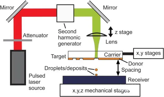
1. Principles and Advantages of LIFT
Laser-Induced Forward Transfer (LIFT) utilizes pulsed lasers (UV-NIR, e.g., 355 nm, 1064 nm) to focus on a donor film, inducing localized phase change or vaporization. The resulting shockwave drives material transfer to a receiver substrate with mICron-scale precision.
Key advantages:
-
High precision: Adjustable laser spot (1–50 μm), ±2 μm transfer resolution;
-
Material versatility: Metals (Au, Cu), dielectrics (PI, BCB), semiconductors (Si), and prefabricated components (e.g., 0201 Resistors/capacitors);
-
Low-temperature compatibility: Suitable for heat-sensitive flexible substrates (PET, PI).
2. Critical Process Steps for Component Embedding
(1) Donor Film Design
-
Structure:
-
Dynamic Release Layer (DRL): Ti, Al, or polyimide (50–200 nm thick) to absorb laser energy;
-
Functional layer: Pre-patterned components/materials (e.g., Cu traces, Si chips).
-
-
Adhesion control:
-
Donor-receiver gap (10–100 μm) to prevent unintended bonding;
-
Receiver suRFace activation (plasma, SAM) for enhanced adhesion.
-
(2) Laser Parameter Optimization
-
Fluence:
-
Threshold: 0.1–5 J/cm², matched to DRL absorption (e.g., α≈10⁶ cm⁻¹ for Ti at 355 nm);
-
Excessive fluence causes thermal damage (carbonization).
-
-
Pulse width:
-
Short pulses (ps/fs) minimize heat diffusion for fine features;
-
Long pulses (ns) enhance shockwaves for larger components.
-
(3) Transfer Dynamics and Precision Control
-
Shockwave modeling:
-
Simulate plasma expansion via hydrodynamic equations (Euler/N-S) to optimize energy distribution;
-
-
Real-time feedback:
-
High-speed CCD (>10⁶ fps) tracks droplet trajectory; PID adjusts laser focus;
-
Confocal displacement sensors (±0.1 μm) compensate substrate roughness.
-
(4) Post-Processing
-
Annealing:
-
200–300°C in N₂ to heal interfacial defects (Cu-Cu contact resistance <10⁻⁸ Ω·m²);
-
-
Interconnects:
-
Laser drilling or damascene plating for vertical connections.
-
3. Core Technical Solutions for High-Precision Embedding
(1) Multi-Layer Heterogeneous Integration
-
Sequential LIFT:
-
Layer-by-layer transfer (e.g., resistors → dielectrics) with ≤±5 μm alignment;
-
Fiducial marks for cross-layer registration.
-
-
3D interconnects:
-
Transfer flip-chip microbumps (≤20 μm diameter, ≤40 μm pitch).
-
(2) Heterogeneous Material Compatibility
-
Thermal stress management:
-
Gradient CTE layers (Si→Cu→PI) suppress delamination under thermal cycling (-55–125°C);
-
FEA optimizes stress distribution (<50 MPa peak).
-
-
Interfacial bonding:
-
Laser-induced alloying (e.g., Au-Sn eutectic) enhances bond strength (>20 MPa).
-
(3) In-Line Inspection and Repair
-
Defect detection:
-
IR thermography for shorts/opens;
-
THz-TDS for non-destructive void detection (≤10 μm resolution).
-
-
Laser repair:
-
Femtosecond laser ablation for defect removal, followed by localized re-deposition.
-
4. Challenges and Solutions
-
Challenge 1: Donor film lifespan:
-
Solution: Roll-to-Roll donor drums or replaceable modules for continuous production.
-
-
Challenge 2: Micro-component transfer stability:
-
Solution: Electrostatic adsorption-assisted LIFT (ESA-LIFT) with 1–10 kV/cm fields.
-
-
Challenge 3: Electrical performance consistency:
-
Solution: SPC + AI models (e.g., Random Forest) to predict/compensate process variations.
-
5. Applications and Validation
-
High-frequency flexible circuits:
-
Embedded GaAs MMICs operating at 40 GHz with <0.5 dB/mm loss;
-
-
3D system-in-package (3D-SiP):
-
Multi-layer interposers with >10⁴ TSVs/cm² and ≥99% yield.
-