 PCB
PCB FPC
FPC Rigid-Flex
 FR-4
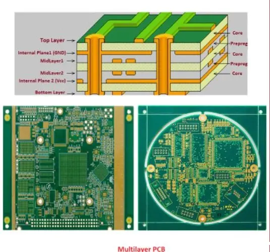
FR-4 HDI PCB
 Rogers High-Frequency Board
 PTFE Teflon High-Frequency Board
 Aluminum
 Copper Core
 PCB Assembly
 LED light PCBA
 Memory PCBA
 Power Supply PCBA
 New Energey PCBA
 Communication PCBA
 Industrial Control PCBA
 Medical Equipment PCBA
 Testing Service
 PCBA Testing Service
 Certification Application
 RoHS Certification Application
 REACH Certification Application
 CE Certification Application
 FCC Certification Application
 CQC Certification Application
 UL Certification Application
 Transformers, Inductors
 High Frequency Transformers
 Low Frequency Transformers
 High Power Transformers
 Conversion Transformers
 Sealed Transformers
 Ring Transformers
 Inductors
 Wires,Cables Customized
 Network Cables
 Power Cords
 Antenna Cables
 Coaxial Cables
 Net Position Indicator
 Solar AIS net position indicator
 Capacitors
 Connectors
 Diodes
 Embedded Processors & Controllers
 Digital Signal Processors (DSP/DSC)
 Microcontrollers (MCU/MPU/SOC)
 Programmable Logic Device(CPLD/FPGA)
 Communication Modules/IoT
 Resistors
 Through Hole Resistors
 Resistor Networks, Arrays
 Potentiometers,Variable Resistors
 Aluminum Case,Porcelain Tube Resistance
 Current Sense Resistors,Shunt Resistors
 Switches
 Transistors
 Power Modules
 Isolated Power Modules
 AC-DC Power Modules
 DC-AC Module(Inverter)
 RF and Wireless
Precision Control of Line Width: The Key to Maintaining RF Microstrip Line Impedance Tolerance within ±3%
In RF PCB design, maintaining controlled impedance in microstrip lines is crucial, and even minor deviations in trace width can significantly impact the characteristic impedance. Generally, for a standard 50Ω microstrip line, if the trace width deviation exceeds approximately ±0.025mm, it can cause the impedance to deviate beyond the acceptable ±3% tolerance (i.e., ±1.5Ω for a 50Ω line) . The exact amount of deviation depends on the specific PCB stack-up, including the dielectric thickness, copper thickness, and the substrate's dielectric constant.
Here is a summary of key relationships and data points:
| Parameter | Typical Influence on Impedance | Notes |
|---|---|---|
| Trace Width (W) | A change of 0.025mm in width can cause a 5-8Ω shift in impedance . | This is a primary factor. For a 50Ω line, this shift already exceeds a ±3% (±1.5Ω) tolerance. |
| Dielectric Thickness (H) | A change of 0.025mm in thickness can cause a 5-8Ω shift in impedance . | Thicker dielectrics lead to higher impedance. |
| Copper Thickness (T) | Thicker copper reduces impedance . Its effect is coupled with line width. | |
| Dielectric Constant (Er) | Varies with material and frequency. Higher Er lowers impedance . |
🔍 How Trace Width Affects Impedance
The width of the trace is a primary determinant of the microstrip line's characteristic impedance. A narrower trace increases impedance, while a wider trace decreases it . This relationship is inverse and non-linear.
-
The Sensitivity to Change: The microstrip impedance structure is quite sensitive. As noted in the search results, a width change of just 0.025mm can lead to an impedance change of 5 to 6 ohms . For a target 50-ohm line, a 6-ohm deviation is a 12% change, far exceeding the typical ±3% (±1.5Ω) control limit.
-
Real-world Manufacturing Tolerances: The allowed variation in trace width during Pcb Production depends on the base copper foil thickness. For example, with 18μm (½ oz) copper, the allowed width tolerance might be around ±0.015mm, while for 35μm (1 oz) copper, it could be about ±0.025mm . This means the inherent manufacturing process can already introduce impedance-varying changes.
📝 Key Influencing Factors in Impedance Control
While trace width is critical, other factors in the PCB stack-up interact with it and contribute to the final impedance value.
-
Dielectric Thickness (H): The distance between the trace and the reference ground plane is another major factor. The impedance is proportional to the natural logarithm of this height . A variation of 0.025mm in dielectric thickness can also cause a 5-8Ω impedance shift . In practice, controlling the laminate and prepreg thickness during lamination is vital for impedance control.
-
Copper Thickness (T): The final thickness of the trace (base copper plus any plating) also affects impedance. Thicker copper lowers the characteristic impedance . This is why plating uniformity is essential, as inconsistencies can lead to localized impedance variations.
-
Dielectric Constant (Er): The dielectric constant of the PCB substrate is not a fixed value; it can vary slightly between material batches and decreases with increasing frequency . This variation must be considered during the initial design calculations.
💡 Practical Guidelines for Robust Design
To ensure your impedance stays within the desired ±3% window, consider the following strategies:
-
Collaborate Early with Your Manufacturer: Before finalizing your design, consult with your PCB fabricator. They can provide their specific capabilities for trace width and dielectric thickness control. Provide them with your desired impedance target and stack-up for feedback .
-
Utilize Impedance Calculation Tools: Use field solvers or industry-proven formulas in tools like Polar Si9000 to accurately model your microstrip line based on your specific stack-up (H, T, Er) . Then, perform a sensitivity analysis by varying the trace width to see its impact.
-
Prioritize a Robust Stack-up: A design that is less sensitive to manufacturing variations is more reliable. If possible, opt for a stack-up where minor changes in width or height do not cause large impedance swings.
-
Specify Impedance Control and Tolerances: Clearly state your impedance requirements and tolerance (e.g., 50Ω ±3%) in your fabrication notes. Also, specify tight tolerances for dielectrics and use low-tolerance materials where critical .
In summary, for RF microstrip lines, maintaining a trace width deviation within approximately ±0.025mm is crucial to keep impedance variation within ±3% for a standard 50-ohm line . Given that standard PCB processes can have trace width tolerances in this range, close collaboration with your PCB manufacturer and careful stack-up design are essential for success.
I hope this detailed explanation helps you in your design. If you have a specific PCB stack-up in mind, I could offer more tailored thoughts.