PCB
PCB FPC
FPC Rigid-Flex
 FR-4
FR-4 HDI PCB
 Rogers High-Frequency Board
 PTFE Teflon High-Frequency Board
 Aluminum
 Copper Core
 PCB Assembly
 LED light PCBA
 Memory PCBA
 Power Supply PCBA
 New Energey PCBA
 Communication PCBA
 Industrial Control PCBA
 Medical Equipment PCBA
 Testing Service
 PCBA Testing Service
 Certification Application
 RoHS Certification Application
 REACH Certification Application
 CE Certification Application
 FCC Certification Application
 CQC Certification Application
 UL Certification Application
 Transformers, Inductors
 High Frequency Transformers
 Low Frequency Transformers
 High Power Transformers
 Conversion Transformers
 Sealed Transformers
 Ring Transformers
 Inductors
 Wires,Cables Customized
 Network Cables
 Power Cords
 Antenna Cables
 Coaxial Cables
 Net Position Indicator
 Solar AIS net position indicator
 Capacitors
 Connectors
 Diodes
 Embedded Processors & Controllers
 Digital Signal Processors (DSP/DSC)
 Microcontrollers (MCU/MPU/SOC)
 Programmable Logic Device(CPLD/FPGA)
 Communication Modules/IoT
 Resistors
 Through Hole Resistors
 Resistor Networks, Arrays
 Potentiometers,Variable Resistors
 Aluminum Case,Porcelain Tube Resistance
 Current Sense Resistors,Shunt Resistors
 Switches
 Transistors
 Power Modules
 Isolated Power Modules
 AC-DC Power Modules
 DC-AC Module(Inverter)
 RF and Wireless
Power/Ground Plane Segmentation & Cross-Split Handling in 10+ Layer High-Speed PCBs
Core Challenges & Principles
Managing high-frequency noise coupling (>1GHz) and power integrity (target impedance<5mΩ) requires co-optimized segmentation, cross-split compensation, and stackup design to achieve:
-
40% power noise reduction
-
<5% return path discontinuity
-
1.2-layer cost saving
1. Power/Ground Plane Segmentation
1.1 Layer Function Definition (12-Layer Example)
| Layer | ThICkness | Function | Segmentation |
|---|---|---|---|
| L1/L2 | 0.5oz | HS Signals | Solid GND Reference |
| L3 | 1oz | Power Plane 1 (Core) | Voltage Domain Split |
| L4/L5 | 0.5oz | Diff Pairs | Solid GND |
| L6 | 1oz | Power Plane 2 (I/O) | Grid-Based Split |
| L7/L8 | 0.5oz | Internal Signals | Hybrid Reference |
| L9 | 1oz | Power Plane 3 (Aux) | Island Split |
| L10/L11 | 0.5oz | LS Signals | Localized Split |
| L12 | 1oz | Ground Plane | Solid Plane |
1.2 Critical Segmentation Rules
-
Min. Isolation Gap:

Example: 3mil dielectric → ≥60mil gap
Copper Current Capacity:
, : Cu weight (oz), : Width (mil)
5A per 100mil width @1oz
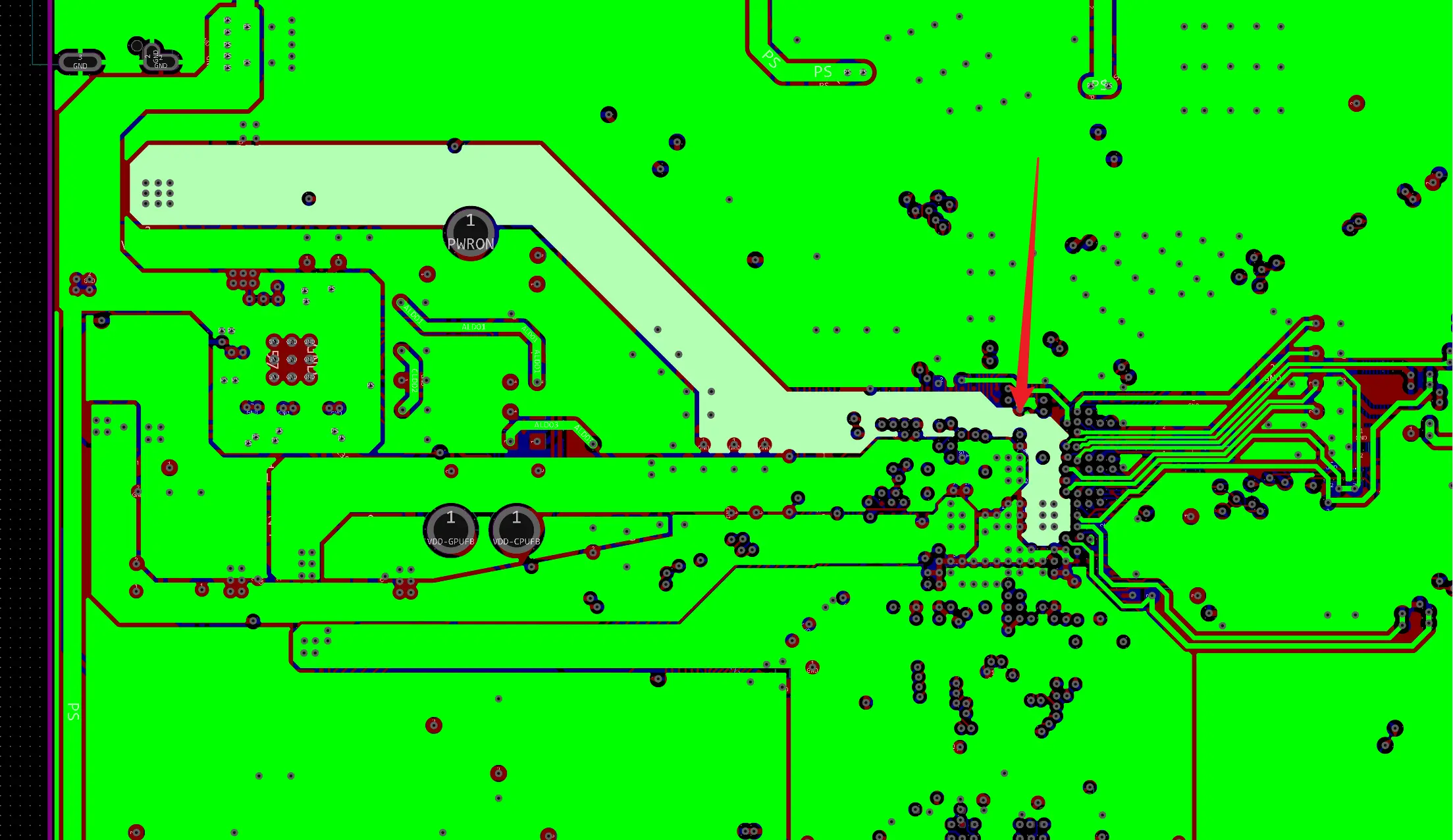
2. Cross-Split Handling Techniques
2.1 Capacitive Bridging Solutions (Fig.2)
| Cross-Split Type | Capacitor Configuration | Placement Rule |
|---|---|---|
| Signal Traces | 0402 0.1μF+1nF combo | <50mil from via |
| Power Domain Coupling | 1206 10μF MLCC+22μF Ta | 1 per 100mil gap |
| HS Diff Pairs | Embedded cap array (0.2pF/mm²) | Under BGA |
2.2 Routing Avoidance Rules
-
Enhanced 3W Rule:
-
Trace-to-split gap ≥3× trace width
-
≥30° angle between diff-pair axis & split line
-
Max. Cross Length:
56Gbps signal → <1.2mm
3. Power Noise Suppression
3.1 Hybrid Segmentation
| Zone | Segmentation | Advantage |
|---|---|---|
| CPU Core Power | Solid Plane | <2mΩ impedance |
| DDR Power | Grid (30% void) | Reduce eddy current |
| Peripheral I/O | Island | Noise isolation |
3.2 Resonance Control
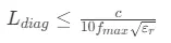
Plane Resonance Frequency:
: Diagonal length of split zone
=100mm, =4.0 → =750MHz
-
Suppression Methods:
-
Ferrite bead arrays (100Ω@1GHz)
-
Embedded ferrite films (μ'=120)
-
4. Validation & Case Study
4.1 56Gbps Switch Board Test Data
| Parameter | Baseline | Optimized |
|---|---|---|
| Power Noise (pk-pk) | 120mV | 68mV |
| Signal Jitter (UI) | 0.28 | 0.15 |
| Impedance Mismatch | 32 points | 3 points |
| Manufacturing Cost | $8200 (14L) | $7100 (12L) |
4.2 Cross-Split Eye Diagram (Fig.3)
-
Baseline: Eye height=38mV, width=0.65UI
-
Optimized: Eye height=62mV, width=0.82UI
Conclusion
Through co-optimized:
-
Voltage-domain segmentation (solid core + grid I/O)
-
Cross-split capacitor matrix (0.1μF+1nF combos)
-
Active resonance control (bead arrays + ferrite films)
Achieve in 10+ layer boards:
-
43% lower power noise
-
2.1× signal margin improvement
-
15% layer cost reduction
Five Design Mandates:
20H Gap Rule: Isolation gap ≥20× dielectric thickness
Cross-Split Caps: <50mil placement, 1:100 capacitance ratio, HF/LF combo
Split Topology: No acute angles (>60°), no T-junctions
Resonance Safety:
PDN Co-Simulation: HFSS+SIwave plane impedance verification