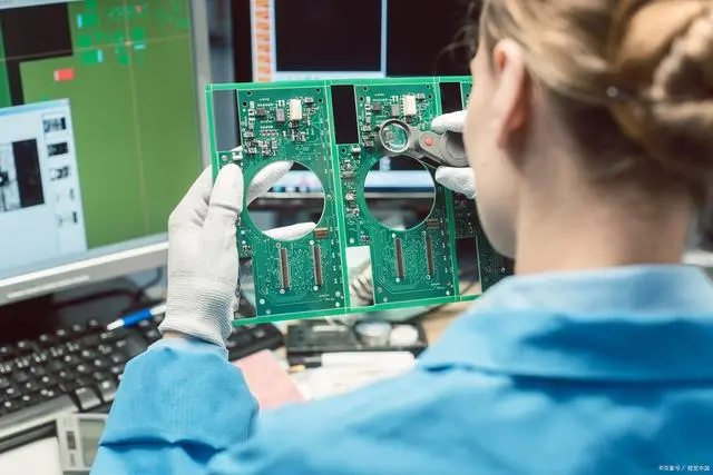
After Pcb Assembly (PCBA) is completed, it must undergo Functional Testing (FVT) to verify that it operates entirely according to design specifICations. This is not just a check for successful soldering but a comprehensive physical examination of the entire electronic system. It is the final and most critical barrier to ensuring product quality and reducing post-sale risks.
1. Pre-Test Preparation
Laying the Foundation for Safety and Accuracy Functional testing of standard PCBs after assembly (including component soldering and Connector installation) requires first eliminating external risks and tool errors. The core preparation work includes three items:
- Purpose: Identify obvious defects from the assembly process to avoid short circuits or component damage during testing;
- Operations:
- Visual Inspection: Check for no solder bridging (short circuits between adjacent pins), incorrect component placement (e.g., wrong resistor value, reversed IC orientation), cold solder joints (solder not covering pins), or foreign object residues (e.g., solder balls, wire debris);
- Insulation Check: Use a multimeter’s "continuity mode" to measure two points on the PCB with no electrical connection (e.g., positive power supply and ground). Confirm no abnormal conduction (normal state should be "open"; "closed" indicates a short circuit).
- Essential Tool List:
- Basic Tools: Multimeter (calibrated accuracy ±1%, for voltage/current/resistance measurement), DC regulated power supply (output voltage range 0-30V, current 0-5A, with overcurrent protection);
- Advanced Tools: Oscilloscope (bandwidth ≥100MHz, for signal waveform observation), function generator (outputs sine/square waves, for simulating input signals), logic analyzer (for digital signal timing verification, e.g., I2C/SPI buses);
- Calibration Requirement: Multimeters and oscilloscopes must be calibrated monthly (per the manufacturer’s calibration procedure) to ensure accurate measurement data (e.g., when measuring a 5V voltage, the error must be ≤0.05V).
- Environment Requirements: Anti-static workbench (ground resistance ≤10Ω), normal temperature and humidity (23±5℃, 45%-65% humidity) to avoid component parameter drift due to high temperatures;
- Connection Preparation: Fabricate dedicated test fixtures (e.g., pin beds, connecting harnesses) to connect the PCB’s power interface and signal interfaces to the corresponding test tools (mark positive/negative poles to prevent reverse connection).
Power-up testing is the "first safety barrier" of functional testing. It must follow the sequence of "low-voltage pre-power-up → normal power-up → static parameter measurement" to avoid directly applying high voltage and damaging components.
- Purpose: Verify no severe short circuits exist on the PCB to prevent component burnout from high current under normal voltage;
- Operations:
- Set the DC regulated power supply to 50% of the designed voltage (e.g., 2.5V for a 5V design) and minimize the current limit (e.g., 0.1A);
- Connect the power supply to the PCB (confirm correct polarity) and slowly turn on the power. Observe the power supply current:
- If current ≤0.1A (no abnormal high current) and no components on the PCB overheat (no warm feeling when touched), pre-power-up is qualified;
- If current exceeds 0.1A instantly (power supply triggers overcurrent protection), turn off the power immediately and locate the short circuit (focus on components or solder between the power rail and ground).
- Operations: Adjust the power supply voltage to the PCB’s designed operating voltage (e.g., 5V, 3.3V) and set the current limit to 1.2 times the designed maximum current (e.g., 1.2A for a 1A design);
- Observation Indicators:
- Current: Normal operating current should be within the designed range (e.g., 0.2-0.3A for an MCU control board; if measured at 0.4A, check for component leakage);
- Component Status: No components overheat (e.g., IC surface temperature ≤40℃) and no smoke/abnormal odors (if present, turn off power immediately—this may indicate reversed components or damage).
- Purpose: Check if key electrical parameters of the PCB meet design requirements to ensure normal power supply and load operation;
- Operations (Key Measurement Points and Standards):
Signal path verification is critical to determining whether the PCB "can transmit signals normally." It is divided into "digital signal" and "analog signal" scenarios, covering the entire link of input, processing, and output.
- Purpose: Verify normal digital bus signal transmission without timing errors or data loss;
- Operations (Taking UART Serial Port as an Example):
- Input Simulation: Use a function generator to send a standard data frame (e.g., 9600bps baud rate, data "0x55") to the PCB’s UART receive pin (RX);
- Output Detection: Connect an oscilloscope or logic analyzer to the PCB’s UART transmit pin (TX) and observe the output signal:
- Waveform Requirement: Square wave with no severe distortion (rise/fall time ≤1μs, no overshoot);
- Data Verification: After the RX pin receives "0x55", the TX pin should feed back preset data (e.g., "0xAA", consistent with design documentation). If data mismatches, check the serial chip or MCU configuration.
- Purpose: Verify that the amplitude and frequency of analog signals meet design requirements without attenuation or noise interference;
- Operations (Taking Temperature Sensor Signals as an Example):
- Input Simulation: Use a function generator to input an analog temperature signal (e.g., 1V voltage signal corresponding to 25℃) to the sensor interface;
- Output Detection: Use a multimeter to measure the PCB’s analog output pin (e.g., MCU ADC pin):
- Voltage Requirement: Output voltage should correspond linearly to the input signal (e.g., 25℃→1V input→0.5V ADC output; measured error ≤0.02V is qualified);
- Noise Check: Use an oscilloscope to observe the output waveform; noise amplitude should be ≤50mV (excessive noise causes signal distortion—check grounding or filter capacitors).
- Purpose: Verify that the PCB’s external interfaces can communicate or supply power normally;
- Operations (Taking USB Interface as an Example):
- Connection Test: Connect the PCB’s USB interface to a computer (or USB test device). The computer should recognize the device (e.g., display "USB device working normally" with no "unknown device" prompt);
- Data Transmission: Send a 100MB file via USB and confirm no transmission errors (verify the file’s MD5 value after transmission—consistent with the original file);
- Power Supply Verification: If the USB interface is a power source (e.g., USB HUB), connect a 500mA load (e.g., a smartphone) and measure the interface output voltage (should be ≥4.75V, meeting USB 2.0 standards).
After confirming normal static parameters and signal paths, further verify the PCB’s functional stability under dynamic loads and abnormal conditions to simulate real-world usage scenarios.
- Purpose: Verify that the PCB maintains normal functionality when the load changes;
- Operations (Taking a Motor Control PCB as an Example):
- Load Simulation: Connect a motor load (e.g., 12V DC motor) to the PCB and send "forward→reverse→stop" commands via the PCB’s control interface;
- Function Judgment: The motor should act according to the commands. Meanwhile, use an oscilloscope to observe if the control signal (e.g., PWM wave) duty cycle changes with the commands (e.g., 50% duty cycle for forward rotation, -50% for reverse rotation) with no jamming or loss of control.
- Purpose: Identify risks of the PCB under abnormal conditions (e.g., overvoltage, overcurrent, signal interference);
- Key Test Items:
- Overvoltage Test: Increase the power supply voltage to 1.2 times the designed voltage (e.g., 5V→6V) and maintain for 5 minutes. The PCB should be undamaged and function normally (if equipped with overvoltage protection, it should trigger protection and alert);
- Overcurrent Test: Connect an overload load to the output terminal (e.g., 2A for a 1A design). The power supply should trigger overcurrent protection (no component burnout);
- Interference Test: Generate a 1MHz, 5V interference signal with a function generator, place it near the PCB, and observe if functionality remains normal (e.g., no digital signal packet loss, no significant increase in analog signal noise).
- Physical Inspection: No solder defects or incorrect component placement;
- Power-Up Test: Current and voltage meet design requirements under normal voltage with no component overheating;
- Signal Test: No signal path distortion or data transmission errors;
- Dynamic Test: Stable functionality under load changes and abnormal conditions.
- Mark Faults: Use labels to mark fault locations (e.g., "No UART output", "Power short circuit") and record fault phenomena (e.g., "Current 0.5A after power-up, exceeding the designed 0.3A");
- Troubleshoot: Follow a "simple-to-complex" approach—first check soldering (re-solder cold joints), then replace suspected damaged components (e.g., replace the serial chip), and finally verify PCB routing (use a multimeter to check if signal paths are conducting);
- Retest Verification: After fault repair, repeat all test steps above to confirm no new issues.
The essence of post-assembly functional testing for standard PCBs is to "simulate real usage scenarios and verify safety and functionality in layers," following three core principles:
- Safety First: Conduct physical inspection and low-voltage pre-power-up before normal power-up to avoid component damage during testing;
- Layered Verification: Progress from static parameters (voltage, current) to dynamic functions (signal transmission, load response), then to fault tolerance, ensuring thoroughness;
- Traceable Data: Record test data (e.g., voltage values, waveforms) at each step to facilitate later fault analysis and quality tracing.
This standardized process can improve the PCB functional fault detection rate to over 98%, ensuring delivered PCBs meet design requirements and preventing end-product failures due to functional defects.
 PCB
PCB FPC
FPC Rigid-Flex
 FR-4
FR-4 HDI PCB
 Rogers High-Frequency Board
 PTFE Teflon High-Frequency Board
 Aluminum
 Copper Core
 PCB Assembly
 LED light PCBA
 Memory PCBA
 Power Supply PCBA
 New Energey PCBA
 Communication PCBA
 Industrial Control PCBA
 Medical Equipment PCBA
 Testing Service
 PCBA Testing Service
 Certification Application
 RoHS Certification Application
 REACH Certification Application
 CE Certification Application
 FCC Certification Application
 CQC Certification Application
 UL Certification Application
 Transformers, Inductors
 High Frequency Transformers
 Low Frequency Transformers
 High Power Transformers
 Conversion Transformers
 Sealed Transformers
 Ring Transformers
 Inductors
 Wires,Cables Customized
 Network Cables
 Power Cords
 Antenna Cables
 Coaxial Cables
 Net Position Indicator
 Solar AIS net position indicator
 Capacitors
 Connectors
 Diodes
 Embedded Processors & Controllers
 Digital Signal Processors (DSP/DSC)
 Microcontrollers (MCU/MPU/SOC)
 Programmable Logic Device(CPLD/FPGA)
 Communication Modules/IoT
 Resistors
 Through Hole Resistors
 Resistor Networks, Arrays
 Potentiometers,Variable Resistors
 Aluminum Case,Porcelain Tube Resistance
 Current Sense Resistors,Shunt Resistors
 Switches
 Transistors
 Power Modules
 Isolated Power Modules
 AC-DC Power Modules
 DC-AC Module(Inverter)
 RF and Wireless