 PCB
PCB FPC
FPC Rigid-Flex
 FR-4
FR-4 HDI PCB
 Rogers High-Frequency Board
 PTFE Teflon High-Frequency Board
 Aluminum
 Copper Core
 PCB Assembly
 LED light PCBA
 Memory PCBA
 Power Supply PCBA
 New Energey PCBA
 Communication PCBA
 Industrial Control PCBA
 Medical Equipment PCBA
 Testing Service
 PCBA Testing Service
 Certification Application
 RoHS Certification Application
 REACH Certification Application
 CE Certification Application
 FCC Certification Application
 CQC Certification Application
 UL Certification Application
 Transformers, Inductors
 High Frequency Transformers
 Low Frequency Transformers
 High Power Transformers
 Conversion Transformers
 Sealed Transformers
 Ring Transformers
 Inductors
 Wires,Cables Customized
 Network Cables
 Power Cords
 Antenna Cables
 Coaxial Cables
 Net Position Indicator
 Solar AIS net position indicator
 Capacitors
 Connectors
 Diodes
 Embedded Processors & Controllers
 Digital Signal Processors (DSP/DSC)
 Microcontrollers (MCU/MPU/SOC)
 Programmable Logic Device(CPLD/FPGA)
 Communication Modules/IoT
 Resistors
 Through Hole Resistors
 Resistor Networks, Arrays
 Potentiometers,Variable Resistors
 Aluminum Case,Porcelain Tube Resistance
 Current Sense Resistors,Shunt Resistors
 Switches
 Transistors
 Power Modules
 Isolated Power Modules
 AC-DC Power Modules
 DC-AC Module(Inverter)
 RF and Wireless
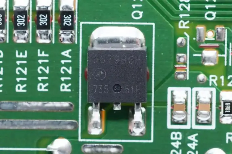
Determining the Matching Relationship Between Heat Dissipating Copper Foil Area and Device Power Consumption in PCB Thermal Design for Power Components (e.g., MOSFETs)
2025-11-08
In PCB design for power electronic systems, thermal management of high-power components like MOSFETs is critical to prevent overheating, ensure long-term reliability, and maintain optimal electrical peRFormance. The heat dissipating copper foil is one of the most cost-effective and widely used passive thermal solutions, and its area must be precisely matched to the device’s power consumption—too small an area leads to excessive temperature rise, while an overly large area wastes PCB space and increases costs. This article details the scientific method for determining this matching relationship, integrating thermal resistance principles, industry standards, test data, and practical design considerations.
1. Core Principles: Thermal Resistance and Temperature Rise Constraints
The matching between copper foil area and device power consumption is rooted in the relationship between thermal resistance, power dissipation, and allowable temperature rise:
- Basic thermal formula: ΔT = P × Rₜₕ, where ΔT is the maximum allowable temperature rise of the device (°C), P is the device’s power consumption (W), and Rₜₕ is the total thermal resistance from the device junction to the ambient environment (°C/W).
- Role of copper foil: The heat dissipating copper foil reduces the thermal resistance between the device’s thermal pad and the ambient (Rₜₕₚₐₙₑₗₐₘᵦᵢₑₙₜ), which is a key component of the total thermal resistance. Increasing the copper foil area decreases Rₜₕₚₐₙₑₗₐₘᵦᵢₑₙₑ, thereby limiting ΔT within the safe range.
- Allowable temperature rise: For MOSFETs, the typical maximum junction temperature (Tⱼₘₐₓ) is 150°C. Assuming an ambient temperature (Tₐ) of 25°C, the allowable temperature rise ΔT = Tⱼₘₐₓ - Tₐ = 125°C. For harsh environments (e.g., automotive underhood, Tₐ = 85°C), ΔT is reduced to 65°C, requiring a larger copper foil area.
2. Standard Matching Guidelines: Copper Foil Area vs. Power Consumption
Based on industry test data (for standard FR-4 PCBs, 1oz/35μm or 2oz/70μm copper foil, natural convection, no heat sink), the following matching relationships are widely recognized for MOSFETs (with thermal pads attached directly to the copper foil):
2.1 1oz Copper Foil (35μm Thickness)
1oz copper is the most common choice for general-purpose PCBs. Its area-power matching is as follows:
- Low power (P ≤ 1W): A 10mm×10mm (100mm²) copper foil area suffices. The thermal resistance Rₜₕₚₐₙₑₗₐₘᵦᵢₑₙₑ is ≈25–30°C/W, leading to a temperature rise of 25–30°C (well within the safe limit).
- Medium power (1W < P ≤ 3W): Requires a 20mm×20mm (400mm²) copper foil. This reduces Rₜₕₚₐₙₑₗₐₘᵦᵢₑₙₑ to 10–15°C/W, limiting ΔT to 30–45°C.
- High power (3W < P ≤ 5W): Needs a 30mm×30mm (900mm²) continuous copper foil. Rₜₕₚₐₙₑₗₐₘᵦᵢₑₙₑ drops to 5–8°C/W, keeping ΔT at 25–40°C.
- Very high power (5W < P ≤ 8W): Requires a 40mm×40mm (1600mm²) copper foil with minimal trace cuts. Rₜₕₚₐₙₑₗₐₘᵦᵢₑₙₑ is 3–5°C/W, ensuring ΔT ≤ 40°C.
2.2 2oz Copper Foil (70μm Thickness)
Thicker copper foil has lower thermal resistance, enabling smaller areas for the same power or higher power handling for the same area:
- Low power (P ≤ 1W): 8mm×8mm (64mm²) is sufficient (Rₜₕₚₐₙₑₗₐₘᵦᵢₑₙₑ ≈18–22°C/W, ΔT = 18–22°C).
- Medium power (1W < P ≤ 3W): 15mm×15mm (225mm²) works (Rₜₕₚₐₙₑₗₐₘᵦᵢₑₙₑ = 7–10°C/W, ΔT = 21–30°C).
- High power (3W < P ≤ 5W): 25mm×25mm (625mm²) is required (Rₜₕₚₐₙₑₗₐₘᵦᵢₑₙₑ = 4–6°C/W, ΔT = 20–30°C).
- Very high power (5W < P ≤ 10W): 35mm×35mm (1225mm²) copper foil (Rₜₕₚₐₙₑₗₐₘᵦᵢₑₙₑ = 2–4°C/W, ΔT = 20–40°C).
2.3 Key Notes on Matching
- The above values assume continuous copper foil (no gaps, slots, or dense trace routing) to maximize heat spreading. Any cuts in the copper foil can increase thermal resistance by 30–50%.
- For multiple MOSFETs mounted on the same PCB, the total copper foil area should be the sum of the individual required areas (with a 10–20% margin) to avoid mutual heat accumulation.
3. Factors Adjusting the Matching Relationship
The standard matching guidelines must be adjusted based on practical design and environmental factors:
3.1 PCB Layer Configuration
- Single-layer PCB: The copper foil is only on one side, so the required area is 30–50% larger than for double-layer PCBs. For example, a 3W MOSFET on a single-layer 1oz PCB needs a 30mm×30mm copper foil (vs. 20mm×20mm for double-layer).
- Multi-layer PCB: Inner copper planes can act as additional heat spreaders. Connecting the top-layer copper foil to inner planes via thermal vias reduces the required top-layer area by 20–30%.
3.2 Environmental Conditions
- Natural convection vs. forced airflow: Forced airflow (e.g., 1m/s fan) reduces thermal resistance by 40–60%, allowing a 30–40% smaller copper foil area. A 5W MOSFET with forced airflow only needs a 20mm×20mm 1oz copper foil (vs. 30mm×30mm for natural convection).
- High ambient temperature: At Tₐ = 85°C, the allowable ΔT is smaller (65°C for MOSFETs), so the copper foil area must be increased by 50–80%. For example, a 3W MOSFET at 85°C requires a 30mm×30mm 1oz copper foil (vs. 20mm×20mm at 25°C).
3.3 Device Mounting and Packaging
- Thermal pad size: MOSFETs with larger thermal pads (e.g., 5mm×5mm vs. 3mm×3mm) transfer heat more efficiently, reducing the required copper foil area by 15–25%.
- Solder paste and thermal interface material (TIM): Using high-thermal-conductivity solder paste (≥50 W/m·K) or TIM (e.g., thermal grease, ≥3 W/m·K) between the thermal pad and copper foil lowers contact resistance, allowing a 10–15% smaller copper area.
4. Practical Calculation Method for Precise Matching
For critical applications requiring precise area determination, follow this step-by-step method:
- Define key parameters: Identify the device’s maximum power consumption (Pₘₐₓ), maximum junction temperature (Tⱼₘₐₓ), ambient temperature (Tₐ), and thermal resistance from junction to case (Rⱼc, provided in the device datasheet).
- Calculate allowable case-to-ambient thermal resistance: Rₙₐₗₗₒwₑd = (Tⱼₘₐₓ - Tₐ) / Pₘₐₓ - Rⱼc.
- Determine copper foil thermal resistance: Rₜₕₚₐₙₑₗₐₘᵦᵢₑₙₑ must be ≤ Rₙₐₗₗₒwₑd. Use industry lookup tables or SIMulation tools (e.g., ANSYS Icepak) to find the copper foil area corresponding to the required Rₜₕₚₐₙₑₗₐₘᵦᵢₑₙₑ.
- Add safety margin: Increase the calculated area by 10–20% to account for manufacturing variations, trace routing, and heat accumulation from adjacent components.
Example Calculation
- MOSFET parameters: Pₘₐₓ = 4W, Tⱼₘₐₓ = 150°C, Tₐ = 25°C, Rⱼc = 2°C/W.
- Allowable Rₙₐₗₗₒwₑd = (150-25)/4 - 2 = 31.25 - 2 = 29.25°C/W.
- For 1oz copper foil, Rₜₕₚₐₙₑₗₐₘᵦᵢₑₙₑ = 6°C/W (25mm×25mm area) ≤ 29.25°C/W.
- With 20% margin: 25mm×1.2 = 30mm → 30mm×30mm (900mm²) copper foil.
5. Best Practices for Optimal Matching
- Maintain copper foil continuity in the heat dissipation area. Avoid routing signal traces through the copper foil; if necessary, use narrow traces (≤0.2mm) and minimize their length.
- For high-power MOSFETs (>5W), combine the copper foil with thermal vias (4–16 filled vias under the thermal pad) to transfer heat to inner layers, reducing the required surface area by 30–40%.
- Use thermal simulation tools (e.g., Cadence Allegro Thermal, Siemens FloTHERM) for complex PCBs with multiple power devices, as they can accurately predict temperature distribution and optimize copper foil area.
- Avoid stacking components directly above or below the heat-dissipating copper foil, as this blocks convection and increases local temperature.
The matching relationship between heat dissipating copper foil area and power consumption in MOSFET PCB thermal design is determined by balancing thermal resistance, allowable temperature rise, and practical constraints. For 1oz copper foil, the area ranges from 100mm² (1W) to 1600mm² (8W) under natural convection, while 2oz copper foil reduces the required area by 20–30% due to lower thermal resistance. Key adjusting factors include PCB layer count, environmental conditions, and device mounting details. By following standard guidelines, using precise calculations, and leveraging simulation tools, designers can achieve an optimal match—ensuring effective heat dissipation without wasting PCB space or increasing costs.