 PCB
PCB FPC
FPC Rigid-Flex
 FR-4
FR-4 HDI PCB
 Rogers High-Frequency Board
 PTFE Teflon High-Frequency Board
 Aluminum
 Copper Core
 PCB Assembly
 LED light PCBA
 Memory PCBA
 Power Supply PCBA
 New Energey PCBA
 Communication PCBA
 Industrial Control PCBA
 Medical Equipment PCBA
 Testing Service
 PCBA Testing Service
 Certification Application
 RoHS Certification Application
 REACH Certification Application
 CE Certification Application
 FCC Certification Application
 CQC Certification Application
 UL Certification Application
 Transformers, Inductors
 High Frequency Transformers
 Low Frequency Transformers
 High Power Transformers
 Conversion Transformers
 Sealed Transformers
 Ring Transformers
 Inductors
 Wires,Cables Customized
 Network Cables
 Power Cords
 Antenna Cables
 Coaxial Cables
 Net Position Indicator
 Solar AIS net position indicator
 Capacitors
 Connectors
 Diodes
 Embedded Processors & Controllers
 Digital Signal Processors (DSP/DSC)
 Microcontrollers (MCU/MPU/SOC)
 Programmable Logic Device(CPLD/FPGA)
 Communication Modules/IoT
 Resistors
 Through Hole Resistors
 Resistor Networks, Arrays
 Potentiometers,Variable Resistors
 Aluminum Case,Porcelain Tube Resistance
 Current Sense Resistors,Shunt Resistors
 Switches
 Transistors
 Power Modules
 Isolated Power Modules
 AC-DC Power Modules
 DC-AC Module(Inverter)
 RF and Wireless
Vias in Power Planes: Aperture Diameter Design to Avoid Current Crowding in PCB Power Distribution Networks
2025-10-28

In PCB power distribution networks (PDNs), power planes (copper layers dedICated to delivering voltage to components) rely on vias to connect to other layers, components, or external power sources. These vias—often called "power vias"—act as critical current pathways, especially in high-current applications like automotive electronics, industrial power supplies, and data center servers.
A major challenge in power via design is current crowding: a phenomenon where current concentrates in narrow regions of the via or its surrounding power plane, leading to three critical issues:
- Increased resistance: Crowded current paths rAISe via resistance (up to 50% higher than designed), causing voltage drops (IR drops) that exceed industry limits (typically ≤5% of the nominal voltage).
- Localized heating: Concentrated current generates excessive heat (Joule heating), with temperatures potentially exceeding 100°C for high-current designs (e.g., 20A power rails), degrading solder joint reliability and PCB substrate integrity.
- Electromigration: High current density (exceeding 1e6 A/cm² for copper) accelerates electromigration (metal ion migration), leading to via failure (open circuits) within 1,000–5,000 hours of operation.
The via aperture diameter—the diameter of the opening in the solder mask (or the via’s conductive barrel, depending on context)—directly determines the via’s current-carrying capacity. Designing the correct aperture diameter is essential to avoid current crowding and ensure PDN stability.
2. Core Principles: Current Capacity and Aperture Diameter Relationship
To define optimal aperture diameters, it first helps to understand how via geometry and current interact, based on industry standards like IPC-2221 and IPC-6012:
2.1 Key Definitions for Power Vias
- Aperture diameter (Dₐ): The diameter of the via’s conductive barrel (for plated-through holes, PTHs) or the solder mask opening (for suRFace-mount power vias). For power vias, this is often used interchangeably with "via diameter" in practical design.
- Current density (J): Current per unit area (A/cm²) flowing through the via. Copper vias have a maximum recommended current density of 1e6 A/cm² for long-term reliability (per IPC standards).
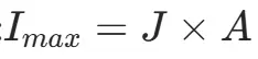
- Current-carrying capacity (Iₘₐₓ): The maximum current a via can safely conduct without crowding, calculated as: Where A is the via’s cross-sectional area (πDₐ²/4, assuming a circular via).
2.2 Factors Influencing Current Crowding Beyond Diameter
While aperture diameter is primary, three factors modify its required size:
- Current magnitude: Higher currents (e.g., 20A vs. 1A) demand larger diameters to keep density below 1e6 A/cm².
- PCB layer stackup: Vias connecting multiple power planes (e.g., a via spanning Layer 1 to Layer 4) require larger diameters than single-layer vias, as current splits across layers.
- Ambient temperature: Elevated temperatures (e.g., 85°C in automotive engine bays) reduce copper’s current-carrying capacity—diameters may need to increase by 10–20% to compensate.
3. Aperture Diameter Design Standards to Avoid Current Crowding
Below are industry-validated aperture diameter guidelines for power vias, organized by current magnitude and aligned with IPC standards. These assume standard copper thickness (35μm, 1oz) and ambient temperatures (25–60°C); adjust for extreme conditions as noted.
3.1 Low-Current Power Vias (≤5A)
Common in low-power electronics (e.g., IoT sensors, consumer wearables) where current demands are minimal:
| Current (I) | Minimum Aperture Diameter (Dₐ) | Cross-Sectional Area (A) | Current Density (J) | Rationale |
|---|---|---|---|---|
| 1A | 0.3mm (12mil) | 0.0707 mm² (0.1096 cm²) | 9.1e4 A/cm² | Well below 1e6 A/cm²; avoids crowding for 1A logic power rails (e.g., 3.3V). |
| 3A | 0.5mm (20mil) | 0.1963 mm² (0.0304 cm²) | 9.87e4 A/cm² | Safely handles 3A for low-voltage power (e.g., 5V USB). |
| 5A | 0.7mm (28mil) | 0.3848 mm² (0.0596 cm²) | 8.39e4 A/cm² | Prevents crowding for 5A power delivery (e.g., small motor drivers). |
Key Note: For 1–5A, even the minimum diameter keeps current density <1e5 A/cm²—far below the electromigration threshold—eliminating crowding risks.
3.2 Medium-Current Power Vias (5–20A)
Typical in industrial controls, automotive infotainment, and mid-power servers, where current demands are moderate:
| Current (I) | Minimum Aperture Diameter (Dₐ) | Cross-Sectional Area (A) | Current Density (J) | Rationale |
|---|---|---|---|---|
| 10A | 1.0mm (40mil) | 0.7854 mm² (0.1217 cm²) | 8.22e4 A/cm² | Handles 10A for 12V automotive power rails without heating (>60°C). |
| 15A | 1.2mm (48mil) | 1.1310 mm² (0.1753 cm²) | 8.56e4 A/cm² | Avoids crowding for 15A industrial power (e.g., 24V sensor arrays). |
| 20A | 1.5mm (60mil) | 1.7671 mm² (0.2739 cm²) | 7.3e4 A/cm² | Safely conducts 20A for mid-power components (e.g., FPGA core power). |
Critical Example: A 20A power via with 1.5mm diameter has a current density of 7.3e4 A/cm²—well below the 1e6 A/cm² limit. Increasing diameter to 1.6mm further reduces density to 6.2e4 A/cm², providing extra margin for temperature fluctuations.
3.3 High-Current Power Vias (>20A)
Found in high-power applications like electric vehicle (EV) charging, server power supplies, and industrial inverters, where current crowding risks are highest:
| Current (I) | Minimum Aperture Diameter (Dₐ) | Cross-Sectional Area (A) | Current Density (J) | Rationale |
|---|---|---|---|---|
| 30A | 2.0mm (80mil) | 3.1416 mm² (0.4869 cm²) | 6.16e4 A/cm² | Prevents crowding for 30A EV auxiliary power (e.g., 12V battery rails). |
| 50A | 2.5mm (100mil) | 4.9088 mm² (0.7609 cm²) | 6.57e4 A/cm² | Handles 50A for server power supplies (e.g., 48V to 12V converters). |
| 100A | 4.0mm (160mil) | 12.5664 mm² (1.9478 cm²) | 5.13e4 A/cm² | Avoids extreme heating (>80°C) for 100A industrial inverters. |
Special Consideration: For >50A, multiple vias (e.g., two 2.5mm vias for 100A) are often used instead of a single large via. This distributes current across the power plane, further reducing crowding and heat.
4. Edge Cases: Adjusting Diameters for Special Scenarios
Certain design constraints or environments require deviations from the baseline diameters. Below are key adjustments:
4.1 High-Temperature Environments (>60°C)
Elevated temperatures reduce copper’s conductivity and current-carrying capacity. For every 10°C increase above 60°C:
- Increase aperture diameter by 10%. For example, a 10A via in an 85°C automotive engine bay (25°C above 60°C) needs a diameter of 1.2mm (up from 1.0mm) to maintain current density <1e5 A/cm².
4.2 Multiple-Layer Power Connections
Vias that connect three or more power layers (e.g., a via linking Layer 1, Layer 3, and Layer 5) split current across layers, but each layer’s via segment still risks crowding. For a 15A via spanning 3 layers:
- Increase diameter by 15% (from 1.2mm to 1.4mm) to ensure each layer’s current segment stays below 5A (15A/3 layers), avoiding localized crowding.
4.3 Space-Constrained Power Planes
In compact PCBs (e.g., wearable medical devices), large vias may not be feasible. Use multiple smaller vias instead:
- Replace one 1.5mm (20A) via with three 0.8mm vias. The total cross-sectional area (3×0.5027 mm² = 1.508 mm²) is similar to the single via, but the smaller diameter fits in tight spaces while avoiding crowding.
5. Validation and Testing of Power Via Diameters
To confirm that aperture diameters avoid current crowding, perform these tests:
5.1 Current Density Simulation (Pre-Layout)
- Use PDN simulation tools (e.g., Cadence Sigrity, ANSYS PowerArtist) to model current flow through the power via and plane.
- Verify that current density across the via is ≤1e6 A/cm² and that no localized hotspots (>60°C) form.
5.2 Physical Current Testing (Post-Production)
- Apply the target current (e.g., 20A) to the power via and measure voltage drop using a precision multimeter.
- Calculate resistance (R = V/I) and confirm it matches the expected value (e.g., ~0.001Ω for a 1.5mm via). Higher resistance indicates current crowding.
5.3 Thermal Imaging (High-Current Vias)
- Use an infrared (IR) camera to capture temperature distribution across the power via and surrounding plane during operation.
- Ensure no localized heating (>80°C) occurs—this is a direct sign of current crowding.
6. Conclusion
The aperture diameter of power vias must be sized to match current demands and avoid current crowding, with core standards based on current magnitude:
- Low current (≤5A): 0.3–0.7mm (12–28mil)
- Medium current (5–20A): 1.0–1.5mm (40–60mil)
- High current (>20A): 2.0–4.0mm (80–160mil)
Adjustments for high temperatures (+10% diameter per 10°C above 60°C), multiple-layer connections (+15% diameter), or space constraints (multiple smaller vias) ensure reliability. By following these guidelines, designers eliminate current crowding, minimize voltage drops, and prevent premature via failure from heating or electromigration.
As power demands grow (e.g., 200A+ in EV main rails), future designs will likely integrate advanced via structures (e.g., buried power vias, copper pillars) with larger effective diameters to maintain current density limits. For now, these diameter standards remain the foundation of robust PDN design.