 PCB
PCB FPC
FPC Rigid-Flex
 FR-4
FR-4 HDI PCB
 Rogers High-Frequency Board
 PTFE Teflon High-Frequency Board
 Aluminum
 Copper Core
 PCB Assembly
 LED light PCBA
 Memory PCBA
 Power Supply PCBA
 New Energey PCBA
 Communication PCBA
 Industrial Control PCBA
 Medical Equipment PCBA
 Testing Service
 PCBA Testing Service
 Certification Application
 RoHS Certification Application
 REACH Certification Application
 CE Certification Application
 FCC Certification Application
 CQC Certification Application
 UL Certification Application
 Transformers, Inductors
 High Frequency Transformers
 Low Frequency Transformers
 High Power Transformers
 Conversion Transformers
 Sealed Transformers
 Ring Transformers
 Inductors
 Wires,Cables Customized
 Network Cables
 Power Cords
 Antenna Cables
 Coaxial Cables
 Net Position Indicator
 Solar AIS net position indicator
 Capacitors
 Connectors
 Diodes
 Embedded Processors & Controllers
 Digital Signal Processors (DSP/DSC)
 Microcontrollers (MCU/MPU/SOC)
 Programmable Logic Device(CPLD/FPGA)
 Communication Modules/IoT
 Resistors
 Through Hole Resistors
 Resistor Networks, Arrays
 Potentiometers,Variable Resistors
 Aluminum Case,Porcelain Tube Resistance
 Current Sense Resistors,Shunt Resistors
 Switches
 Transistors
 Power Modules
 Isolated Power Modules
 AC-DC Power Modules
 DC-AC Module(Inverter)
 RF and Wireless
PCB Pad Design Compatibility and SMT Soldering Reliability Verification for FCQFN and WLCSP Packages Introduction to WLCSP
2026-01-16
PCB Pad Design Compatibility and SMT Soldering Reliability VerifICation for FCQFN and WLCSP Packages
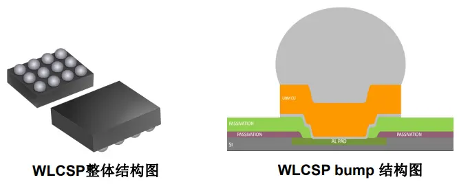
Introduction to WLCSP Wafer Level Chip Scale Packaging (WLCSP) is a packaging method where the package volume is essentially equal to the original size of the IC die. Unlike traditional packaging methods (which involve dicing the wafer first and then packaging, typically increasing the volume by at least 20%), this advanced technology involves packaging and testing the entire wafer first before dicing it into individual IC chips. The WLCSP structure consists of four parts: the Silicon Die, Re-passivation, UBM (Under Bump Metallurgy), and Solder Balls (bumps). The chip connects to the outside world by directly mounting solder balls onto the silicon substrate. The structure is illustrated in Figure 1.
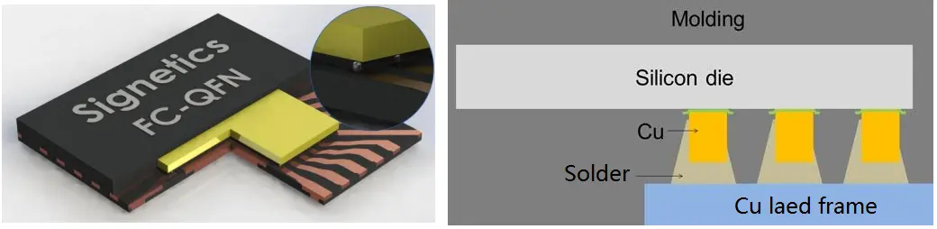
Introduction to FCQFN Flip Chip Quad Flat No-lead Packaging (FCQFN), also known as Flip Chip on Leadframe, is an advanced packaging technology developed from the standard QFN. The chip is mounted face-down, connecting directly to the terminals on the leadframe via bumps. It features an exposed pad (EP) on the bottom for enhanced thermal dissipation. The structure is illustrated in Figure 2.
Comparison of FCQFN vs. WLCSP Compared to WLCSP packaging, FCQFN offers the following advantages:
- Stress Resistance: FCQFN chips are encapsulated in resin, providing better resistance to mechanical stress compared to the unencapsulated WLCSP.
- Ease of Repair: The rigid leadframe of FCQFN provides a stable support base during rework, preventing the damage often caused by improper handling of WLCSP chips.
- Reworkability: FCQFN chips can be re-used after removal and re-balling, whereas WLCSP chips are typically destroyed during rework and cannot be reused.
- Reliability: FCQFN demonstrates superior reliability in tests such as Drop Tests and Bending Tests.
- Manufacturing Yield: FCQFN chips are taped and shipped immediately after testing. In contrast, WLCSP chips undergo back-grinding, marking, dicing, and taping after testing, exposing them to a higher risk of damage and failure.
- Thermal PeRFormance: Thanks to the metal leadframe, FCQFN offers better heat dissipation than WLCSP.
Due to the relatively high production cost of WLCSP, there is a demand to replace WLCSP products with FCQFN to reduce costs. While foundries achieve this through new leadframe and chip designs, our focus is on verifying the compatibility of the application-side PCB pad design and assembly process.
Compatible Pad Design for WLCSP and FCQFN
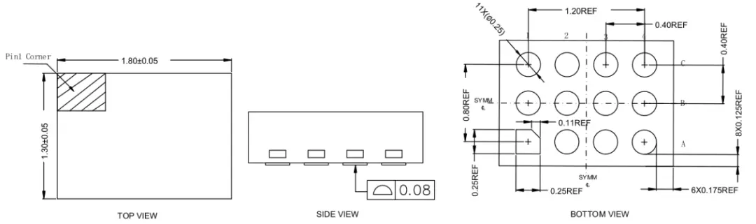
- WLCSP Device:A port protection Switch from a specific manufacturer was selected.
- Part Number: WLCSP 1.82X1.27-12B
- Pitch: 0.4mm
- Ball Diameter: 0.268 ± 0.020mm
- Ball Height: 0.195 ± 0.020mm

- FCQFN Device: An over-voltage protection load switch from the same manufacturer was selected.
- Part Number: FCQFN 1.8 × 1.3 -12
- Pitch: 0.4mm
- Bottom Pad Size: ∅0.25mm
- First Pin: Square 0.25mm with chamfer.
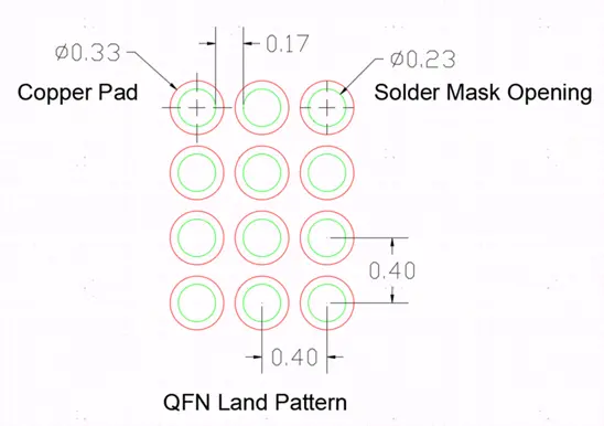
- Pad Design: Compatible pads for WLCSP and FCQFN can be designed using either the Non-Solder Mask Defined (NSMD) or Solder Mask Defined (SMD) method.
- Test Design: NSMD was adopted for this experiment.
- Pad Size: ∅0.23mm
- Solder Mask Opening: ∅0.33mm
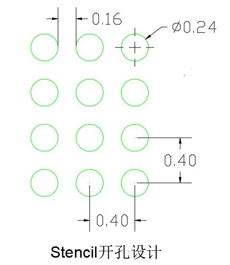
Compatible Stencil Design For CSP or QFN packages with a 0.4mm pitch, the standard stencil thickness ranges from 0.08mm to 0.10mm, with an aperture size of 0.23mm to 0.24mm.
- Test Stencil: FG Nano stencil.
- Thickness: 0.08mm
- Aperture Size: ∅0.24mm
Experimental Plan
- Samples & Parameters: 500 units of WLCSP and 500 units of FCQFN were used. Both utilized identical PCB designs (0.23mm diameter NSMD pads) and stencils (0.08mm thickness, 0.24mm aperture). Placement and soldering parameters matched standard production settings.
- Cross-Section Verification: Post-SMT samples were cross-sectioned to inspect the soldering condition and stand-off height.
- Reliability Testing: 80 functional units of each package were subjected to 300 cycles of Thermal Shock (TST) and 1000 cycles of Temperature Cycling (TCT).
- Reliability Analysis: Post-test samples were cross-sectioned again to check for changes in the solder joints.
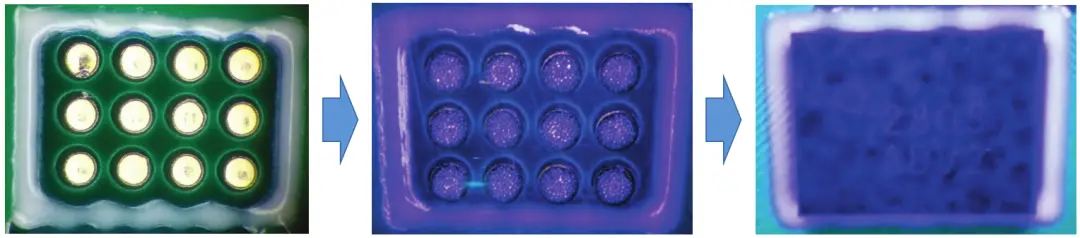
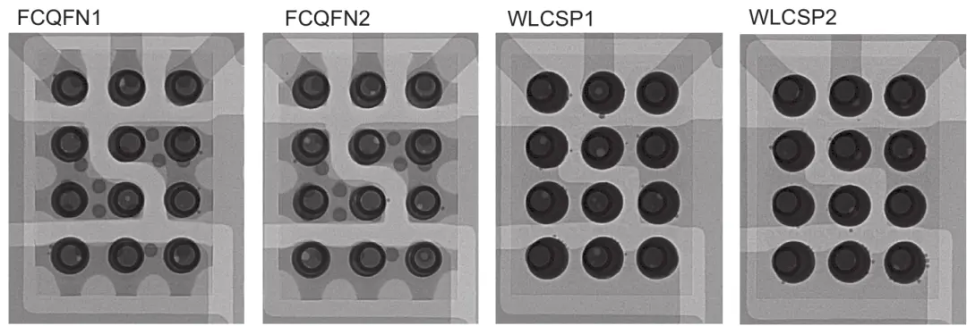
Solder Joint Quality Confirmation - X-RAY & Cross Section
- X-Ray Inspection: 10 units of each package were inspected. No open circuits, short circuits, or excessive voids (>25%) were found. Minor placement offsets were observed but were within acceptable limits (less than the minimum ball pitch).
- Conclusion: Soldering results are OK.
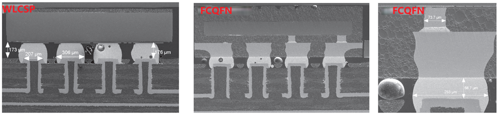
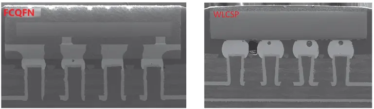
- Cross-Section Analysis:
- WLCSP: Post-reflow stand-off height was approximately 175um, with a solder joint diameter of about 306um. (Pre-reflow: Height 195um, Diameter 268um). The solder balls collapsed, resulting in a final height lower than the original diameter.
- FCQFN: Post-reflow stand-off height was approximately 67um, with a solder joint diameter of about 253um. (Pre-reflow: Paste height 0-50um, Diameter ~250um). The leads were raised, resulting in a final height higher than the original paste height.
- Conclusion: Soldering results are OK.
Package Reliability Verification - TST300 & TCT1000
- TST 300 Cycles: 80 units each of FCQFN and WLCSP underwent Thermal Shock Testing (-45°C to 125°C). The test evaluates resistance to thermal stress. All units passed performance testing after 300 cycles.
- TCT 1000 Cycles: 80 units each underwent Temperature Cycle Testing (-45°C to 125°C). All units passed performance testing after 1000 cycles.
Post-Reliability Cross-Section Confirmation Cross-sections of samples after the TST 300 cycle test confirmed the solder joint status. The images showed no obvious changes or damage to the solder joints.
Summary In this case study, FCQFN packages were successfully assembled using the exact same PCB pads and stencil design as WLCSP. The soldering results were qualified, achieving compatibility in design and manufacturing while meeting high reliability standards. This provides strong empirical data support for compatible design solutions.
Side Note: To maintain flexibility in using components with different packages, pinouts, or from different vendors without changing the PCB layout or fabricating new boards, we often adopt compatible pad designs. This is a strategic engineering approach to improve design flexibility, mitigate supply chain risks, accelerate product iteration, and reduce costs. It embodies the strategy of "trading design complexity for maximum flexibility throughout the product lifecycle." Compatible pad design requires finding the optimal balance between "design flexibility" and "manufacturing reliability and cost." It is essentially a calculated art of compromise.