 PCB
PCB FPC
FPC Rigid-Flex
 FR-4
FR-4 HDI PCB
 Rogers High-Frequency Board
 PTFE Teflon High-Frequency Board
 Aluminum
 Copper Core
 PCB Assembly
 LED light PCBA
 Memory PCBA
 Power Supply PCBA
 New Energey PCBA
 Communication PCBA
 Industrial Control PCBA
 Medical Equipment PCBA
 Testing Service
 PCBA Testing Service
 Certification Application
 RoHS Certification Application
 REACH Certification Application
 CE Certification Application
 FCC Certification Application
 CQC Certification Application
 UL Certification Application
 Transformers, Inductors
 High Frequency Transformers
 Low Frequency Transformers
 High Power Transformers
 Conversion Transformers
 Sealed Transformers
 Ring Transformers
 Inductors
 Wires,Cables Customized
 Network Cables
 Power Cords
 Antenna Cables
 Coaxial Cables
 Net Position Indicator
 Solar AIS net position indicator
 Capacitors
 Connectors
 Diodes
 Embedded Processors & Controllers
 Digital Signal Processors (DSP/DSC)
 Microcontrollers (MCU/MPU/SOC)
 Programmable Logic Device(CPLD/FPGA)
 Communication Modules/IoT
 Resistors
 Through Hole Resistors
 Resistor Networks, Arrays
 Potentiometers,Variable Resistors
 Aluminum Case,Porcelain Tube Resistance
 Current Sense Resistors,Shunt Resistors
 Switches
 Transistors
 Power Modules
 Isolated Power Modules
 AC-DC Power Modules
 DC-AC Module(Inverter)
 RF and Wireless
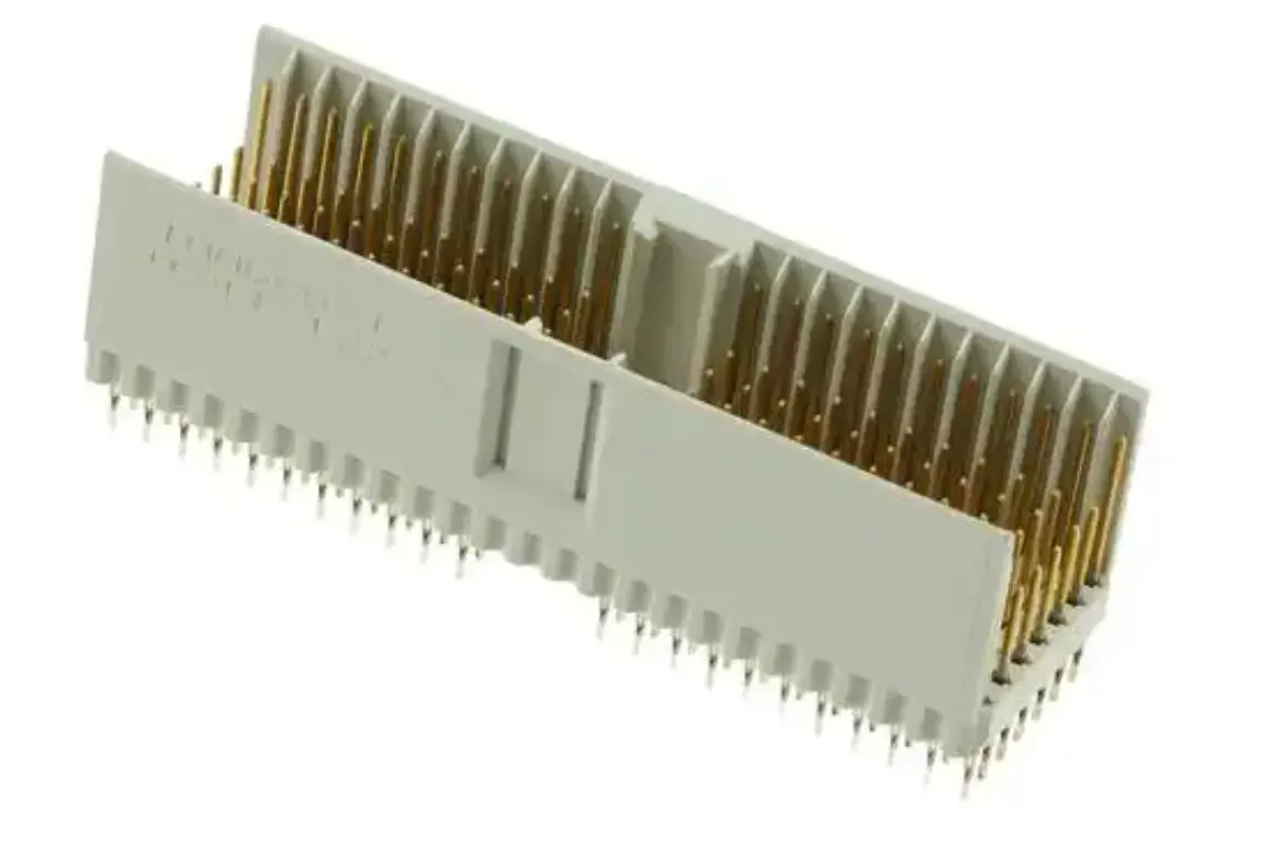
PCB Hole Tolerance Design for Press-Fit Connector Assembly
Introduction
Press-fit Connectors, valued for solderless reliability, are widely used in automotive and industrial electronics. Their electrical connection relies on elastic deformation between metal pins and plated through holes (PTHs), where hole tolerance design critically impacts insertion force, contact resistance, and long-term durability. This article systematically explains design principles and validation methods from mechanical inteRFerence theory, material compatibility, and manufacturing perspectives.
1. Working Principles and Design Requirements
1.1 Mechanical Interference Mechanism
The interference () between pin and hole is calculated as:

where:
-
: Nominal pin diameter (including plating, e.g., Sn or Au)
-
: PCB drilled hole diameter (post-plating)
Typical interference ranges from 0.05-0.15mm. Insufficient interference causes poor contact, while excessive values risk PCB delamination.
1.2 Key Performance Metrics
-
Insertion force: Proportional to interference, typically <50N/pin;
-
Contact resistance: <10mΩ (per IEC 60512);
-
Retention force: Axial pull force >20N (vibration resistance).
2. PCB Hole Tolerance Design Guidelines
2.1 Baseline Hole Diameter Calculation
Determine nominal hole diameter () from connector datasheets:
Example: For an automotive connector with and :
2.2 Tolerance Band Allocation
Considering PCB drilling tolerance (±0.05mm) and pin diameter variation (±0.02mm), total tolerance bandwidth () should satisfy:
Asymmetric tolerance is recommended (Figure 2):
-
Upper limit: +0.03mm (prevent over-interference)
-
Lower limit: -0.07mm (compensate copper plating)
3. Material and Process Considerations
3.1 PCB Substrate Selection
-
High-Tg materials: FR-4 Tg≥170℃ minimizes hole deformation under thermal cycling;
-
Copper thickness control: 25-35μm plating thickness balances mechanical strength and hole size.
3.2 Critical Manufacturing Processes
-
Drilling precision: Laser drilling (±0.025mm) or mechanical drilling (±0.05mm);
-
Plating uniformity: Pulse plating ensures ≤±5% thickness variation;
-
Deburring: Chemical etching or plasma cleaning achieves hole edge R-angle <0.02mm.
4. Validation and Testing Methods
4.1 Mechanical Simulation
-
FEA model (Figure 3):
-
Pin material: Phosphor bronze (E=110GPa);
-
PCB substrate: Anisotropic composite (E_z=6GPa);
-
-
Outputs:
-
Max stress <200MPa (avoid FR-4 cracking);
-
Plastic deformation rate <5% (elastic contact).
-
4.2 Physical Testing
-
Insertion force profiling: Monitor force-displacement curve for smooth transitions;
-
Micro-ohm testing: Measure inter-pin resistance (std. deviation <0.5mΩ);
-
Thermal shock testing: -40℃~+125℃ for 1000 cycles, hole diameter change <2%.
5. Case Study: Automotive BMS Design
Parameters for a battery management system:
-
Connector: TE 3-1773830-2 (pin Ø1.6mm);
-
PCB hole: 1.42±0.04mm (post-plating 1.38-1.46mm);
-
Results: 28N/pin insertion force, <3% resistance increase after 200 mating cycles.