 PCB
PCB FPC
FPC Rigid-Flex
 FR-4
FR-4 HDI PCB
 Rogers High-Frequency Board
 PTFE Teflon High-Frequency Board
 Aluminum
 Copper Core
 PCB Assembly
 LED light PCBA
 Memory PCBA
 Power Supply PCBA
 New Energey PCBA
 Communication PCBA
 Industrial Control PCBA
 Medical Equipment PCBA
 Testing Service
 PCBA Testing Service
 Certification Application
 RoHS Certification Application
 REACH Certification Application
 CE Certification Application
 FCC Certification Application
 CQC Certification Application
 UL Certification Application
 Transformers, Inductors
 High Frequency Transformers
 Low Frequency Transformers
 High Power Transformers
 Conversion Transformers
 Sealed Transformers
 Ring Transformers
 Inductors
 Wires,Cables Customized
 Network Cables
 Power Cords
 Antenna Cables
 Coaxial Cables
 Net Position Indicator
 Solar AIS net position indicator
 Capacitors
 Connectors
 Diodes
 Embedded Processors & Controllers
 Digital Signal Processors (DSP/DSC)
 Microcontrollers (MCU/MPU/SOC)
 Programmable Logic Device(CPLD/FPGA)
 Communication Modules/IoT
 Resistors
 Through Hole Resistors
 Resistor Networks, Arrays
 Potentiometers,Variable Resistors
 Aluminum Case,Porcelain Tube Resistance
 Current Sense Resistors,Shunt Resistors
 Switches
 Transistors
 Power Modules
 Isolated Power Modules
 AC-DC Power Modules
 DC-AC Module(Inverter)
 RF and Wireless
How to Avoid Pad Lifting Caused by Repeated Heating During Manual Touch-Up Soldering
2026-01-01
Manual touch-up soldering is an indispensable skill in electronic manufacturing, repair, and maintenance, serving critical roles in rectifying soldering defects, replacing faulty components, and modifying Circuit Board layouts. However, pad lifting—defined as the detachment of copper pads from the printed circuit board (PCB) substrate—remains a pervasive and costly issue, particularly when repeated heating cycles are required. This phenomenon not only renders the affected pad inoperable but can also damage adjacent traces, vias, and the PCB substrate itself, compromising product reliability, increasing repair costs, and delaying production schedules.
The root cause of pad lifting from repeated heating lies in the inherent mismatch of thermal expansion coefficients (CTE) between the PCB’s constituent materials and the cumulative thermal stress induced by cyclic heating and cooling. A typical PCB comprises a substrate (most commonly FR-4, a glass fiber-reinforced epoxy resin), copper pads/traces, and a solder mask. Copper exhibits a significantly higher CTE (approximately 16.5 × 10⁻⁶/°C) than FR-4 (12 × 10⁻⁶/°C in the x-y plane). When heated, these materials expand at disparate rates; upon cooling, they contract unevenly. Repeated cycles of expansion and contraction generate persistent tensile and shear stresses at the copper-substrate inteRFace, where bonding relies on mechanical adhesion and chemical interactions. Over time, these stresses exceed the interface’s bonding strength, leading to gradual delamination. Compounding this issue are improper soldering practices—such as excessive temperature, prolonged heating, incorrect heat application, or inappropriate flux use—which accelerate stress accumulation and increase the likelihood of pad lifting even with fewer heating cycles.
Mitigating pad lifting during manual touch-up soldering requires a systematic, multi-stage approach encompassing pre-soldering preparation, strategic tool and material selection, standardized operational techniques, precise heating parameter control, and post-soldering inspection. Each stage is interconnected, and strict adherence to best practices across all phases is essential to minimize thermal stress and preserve pad integrity.
Pre-Soldering Preparation: Establish a Foundation for Success
Thorough pre-soldering preparation is the cornerstone of avoiding pad lifting, as it reduces the need for repeated heating by optimizing the soldering environment, identifying potential risks, and ensuring component and PCB compatibility. This phase encompasses PCB inspection and pretreatment, component preparation, and tool calibration.
PCB Inspection and Pretreatment
A comprehensive PCB inspection prior to soldering is critical to identifying vulnerabilities that may exacerbate pad lifting. Begin with a visual assessment: examine the solder mask for cracks, peeling, or discoloration, which indicate substrate damage or prior thermal stress. Inspect copper pads for signs of oxidation, corrosion, or initial delamination—even minor oxidation weakens the solder joint and increases heating requirements. For slightly oxidized pads, apply a small amount of flux and gently wipe the surface with a clean, low-temperature soldering iron tip to remove oxides; severely oxidized or corroded pads should be replaced if possible, as repeated heating will further compromise their bonding strength.
Next, verify PCB specifications, including substrate material and copper layer thickness. FR-4 is standard, but high-temperature applications may use polyimide or ceramic substrates, which exhibit different thermal stability. Copper layer thickness (typically 0.5oz to 2oz) impacts heat conduction and stress resilience: thicker copper (2oz) dissipates heat better but generates greater thermal expansion forces, while thinner copper (0.5oz) is more susceptible to deformation under stress. For PCBs with thin copper layers or fragile substrates, stricter heating controls are necessary.
Appropriate PCB preheating is a key pretreatment step that minimizes thermal stress. Preheating the entire PCB to a uniform temperature (80–120°C for FR-4) reduces the temperature gradient between the local pad and the substrate during soldering, mitigating differential expansion. Use a hot plate, infrared preheater, or dedicated PCB fixture for preheating, ensuring even heat distribution over 2–5 minutes. Avoid excessive preheating, as temperatures above 120°C can damage the substrate or pre-mounted components.
Component Preparation
Proper component preparation eliminates soldering errors that would require repeated heating. First, confirm component compatibility: verify that the component’s model, pin size, and pitch match the PCB’s pad design. Mismatched components force repositioning and re-soldering, increasing thermal stress. Next, pretreat component pins: remove oxides and contaminants using fine-grit sandpaper (400–600 mesh) or a pin cleaner, then tin the pins with a thin, uniform layer of solder. Tinning improves solder wettability, shortens soldering time, and reduces heating cycles. Control tinning temperature at 300–320°C to avoid pin damage, and ensure the tin layer is thin enough to prevent excessive solder accumulation on the pad.
For reused components (e.g., in repair scenarios), inspect pins for bending, deformation, or damage, and straighten or replace them as needed. Use fixtures (e.g., PCB clamps, tweezers) to align components with pads precisely before soldering, preventing displacement that would necessitate re-heating and rework.
Tool Calibration and Setup
Stable, calibrated tools are essential for precise heating control. The core tool—an electric soldering iron equipped with a temperature-controlled soldering station—must maintain accurate temperatures. Calibrate the soldering iron using a temperature tester before use: heat the iron to the desired temperature, stabilize for 5–10 minutes, and verify the tip temperature (error margin ±5°C). Adjust or service the soldering station if calibration fails.
Select a soldering iron tip that matches the pad size and component pins. For small pads (e.g., 0402, 0603 packages), use a pointed or conical tip (0.5mm diameter) for targeted heating; for larger pads (e.g., QFP, BGA peripheries), use a chisel-shaped or rectangular tip (1.5×3mm) to increase contact area, improve heat transfer, and reduce heating time. Keep the tip clean and tinned: wipe with a damp sponge to remove oxides and solder residues, then apply a thin solder layer to enhance thermal conductivity. A dirty or oxidized tip reduces heat transfer efficiency, prolonging heating and increasing the need for repeated cycles.
Prepare auxiliary tools, including flux applicators, solder wire holders, desoldering tools (desoldering pumps, wick), and heat shields. Inspect desoldering tools to ensure functionality, as improper desoldering (e.g., excessive heating) is a leading cause of pad lifting.
Tool and Material Selection: Optimize Compatibility and Performance
The choice of soldering materials (solder wire, flux) and tools directly impacts heating requirements and pad stress. Inferior or mismatched materials increase soldering difficulty, extend heating time, and elevate pad lifting risk.
Solder Wire Selection
Solder wire composition and diameter determine soldering temperature, wettability, and joint quality. For manual touch-up soldering, use RoHS-compliant lead-free solder wire, typically Sn-Ag-Cu (SAC) alloys. SAC305 (Sn96.5/Ag3.0/Cu0.5) is widely preferred, with a melting point of ~217°C—higher than traditional Sn63/Pb37 (183°C) but offering superior mechanical strength and corrosion resistance. When using lead-free solder, adjust the soldering temperature appropriately (340–360°C for SAC305) but avoid exceeding 380°C, as excessive heat accelerates pad delamination.
Match solder wire diameter to pad size: use 0.3–0.4mm diameter for small pads and fine-pitch components (0.5mm pitch QFP) to ensure precise solder application and avoid short circuits. For larger pads, 0.5–0.6mm diameter wire improves efficiency. Select solder wire with 1.0–3.0% flux content (by weight); flux removes oxides, enhances wettability, and promotes joint formation. Excessive flux leaves residues that may corrode pads over time, while insufficient flux increases soldering difficulty and heating requirements. Store solder wire in a dry, cool environment to prevent moisture absorption, which causes spattering during soldering and may require rework.
Flux Selection
Flux is critical for reducing soldering temperature and time, thereby minimizing thermal stress. Choose flux based on activity level: low-activity (RMA) flux is ideal for most applications, offering moderate oxide removal, minimal residues, and low corrosion risk. Medium-activity (RA) or high-activity (R) flux may be used for severely oxidized pads but requires thorough post-soldering cleaning with anhydrous ethanol or dedicated flux cleaner to prevent residue-induced corrosion. Ensure flux compatibility with the PCB substrate and solder mask to avoid chemical damage.
Apply flux sparingly and evenly using a flux applicator or small brush. Excessive flux causes uncontrolled solder spread, requiring repeated heating to correct; insufficient flux leads to poor wettability and prolonged heating. For fine-pitch components, use no-clean flux to eliminate cleaning-related rework and additional heating.
Auxiliary Tool Selection
Auxiliary tools reduce thermal stress and improve soldering precision. PCB fixtures secure the board during soldering, preventing movement that causes errors and rework. Heat shields (metal or high-temperature plastic) protect adjacent components and traces from heat radiation, critical for dense PCB layouts. For large components or multi-pad soldering, combine a soldering iron with a hot air gun: the hot air gun provides uniform heating to the component area, reducing local thermal stress, while the soldering iron targets individual pads for precise solder application.
Desoldering tools must be selected carefully to avoid pad damage. Use desoldering wick (copper braid) with flux for small pads: apply the wick to the pad, heat gently with the soldering iron, and allow the wick to absorb molten solder. For larger pads, use a desoldering pump (solder sucker): heat the pad to melt solder, then activate the pump to remove it. Avoid excessive heating during desoldering—limit each cycle to 2–3 seconds, and allow the pad to cool before reattempting.
Standardized Soldering Operations: Minimize Thermal Stress
Proper soldering technique is the most direct way to avoid pad lifting from repeated heating. Standardized operations focus on minimizing heating time, applying heat uniformly, and avoiding unnecessary rework.
Heat Application Technique
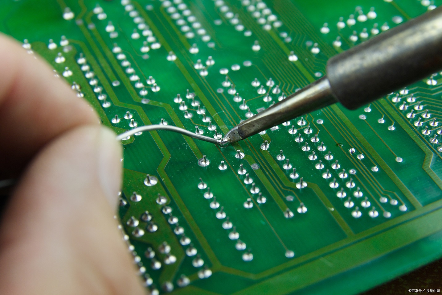
The key to reducing thermal stress is to apply heat efficiently and uniformly. For individual pads, position the soldering iron tip to contact both the pad and the component pin simultaneously—this ensures heat is transferred to both surfaces, melting solder quickly and reducing heating time. Avoid heating only the pad or pin, as this prolongs the soldering cycle and increases stress.
Limit each soldering cycle to 2–3 seconds for small pads and 3–5 seconds for large pads. Exceeding these times causes excessive substrate heating and accelerates pad delamination. If the solder does not melt within the time limit, remove the iron, allow the pad to cool (30–60 seconds), reapply flux, and retry. Never apply excessive pressure to the pad with the soldering iron tip—this damages the copper-substrate bond and increases lifting risk.
For multi-pad components (e.g., SOIC, QFP), use a "drag soldering" technique: heat one end pad, apply solder to form a joint, then drag the soldering iron tip along the row of pads, applying a small amount of solder as needed. This reduces the number of heating cycles per pad and ensures uniform joint formation. For fine-pitch components, follow with a "wicking" step to remove excess solder, using minimal heat to avoid reworking joints.
Avoiding Repeated Heating Cycles
Repeated heating is the primary driver of pad lifting, so minimizing rework is critical. Ensure component alignment before soldering—use tweezers to hold components in place and verify alignment under a magnifying glass. Apply the correct amount of solder in a single cycle: insufficient solder requires re-heating to add more, while excessive solder necessitates wicking (and additional heating) to remove.
If a solder joint is defective (e.g., cold joint, short circuit), allow the pad to cool completely (1–2 minutes) before reworking. Rapid re-heating increases thermal stress by preventing full contraction of the copper and substrate. When reworking, apply a small amount of fresh flux to improve wettability and reduce heating time.
Desoldering Best Practices
Desoldering is a high-risk operation for pad lifting, as it often requires repeated heating. When removing components, use the minimum heat necessary to melt solder. For through-hole components, heat the pad from the top while pushing the pin from the bottom to release it—avoid twisting or pulling the pin, as this damages the pad. For surface-mount components (SMDs), use a hot air gun to heat the entire component uniformly (300–320°C) until the solder melts, then lift the component with tweezers. Avoid localized heating of individual pads during SMD removal, as this creates uneven stress.
After desoldering, inspect the pad for damage. If the pad is intact but has solder residues, clean it with flux and a soldering iron tip (low temperature) to remove debris. If the pad shows signs of delamination (e.g., lifting edges), stop soldering immediately and repair the pad using a copper tape or conductive epoxy.
Heating Parameter Control: Precision is Key
Accurate control of soldering temperature and heating time is critical to minimizing thermal stress. The optimal temperature depends on the solder type, component, and PCB substrate:
- Lead-free solder (SAC305): 340–360°C. Avoid exceeding 380°C, as this degrades the PCB substrate and weakens pad bonding.
- Lead-based solder (Sn63/Pb37): 300–320°C. Lower temperatures reduce thermal stress but require sufficient flux for good wettability.
- Heat-sensitive components (e.g., capacitors, LEDs): Use the minimum temperature required to melt solder, and limit heating time to 2 seconds per pad. Use a heat sink (e.g., alligator clip) attached to the component lead to dissipate heat and protect the component.
Monitor the soldering iron temperature continuously during operation. Temperature fluctuations (common with uncalibrated tools) increase the need for repeated heating, so use a soldering station with real-time temperature feedback. Avoid touching the soldering iron tip to the PCB substrate, as this causes localized overheating and substrate damage.
Post-Soldering Inspection and Maintenance: Preserve Pad Integrity
Post-soldering inspection identifies potential pad damage and ensures joint quality, preventing future failures that would require rework and repeated heating. Inspect each solder joint under a magnifying glass (10–20x magnification) for:
- Pad integrity: Check for lifting edges, delamination, or discoloration (signs of overheating).
- Solder joint quality: Ensure the joint is smooth, shiny, and forms a concave fillet between the pad and component pin. Avoid cold joints (dull, grainy appearance) or excessive solder (bulky, irregular shape), which may require rework.
- Residues: Remove flux residues with a compatible cleaner if using non-no-clean flux. Residue buildup can cause corrosion and weaken pad bonding over time.
If a pad is damaged (e.g., partial lifting), repair it immediately to avoid further degradation. For minor lifting, apply a small amount of conductive epoxy to reattach the pad to the substrate, then cure the epoxy according to the manufacturer’s instructions. For severe damage, replace the pad using copper tape: cut the tape to match the pad size, attach it to the substrate, and solder the component to the new pad.
Store repaired PCBs in a dry, static-free environment to prevent moisture absorption and electrostatic damage, which can compromise pad integrity and require additional rework.
Conclusion
Pad lifting caused by repeated heating during manual touch-up soldering is a preventable issue that requires a systematic approach to minimize thermal stress and optimize soldering practices. By prioritizing pre-soldering preparation (inspection, pretreatment, calibration), selecting compatible tools and materials (solder wire, flux, auxiliary tools), following standardized soldering and desoldering techniques, controlling heating parameters precisely, and conducting thorough post-soldering inspection, technicians can significantly reduce the risk of pad lifting.
The key principle underlying all these practices is to minimize the number and intensity of heating cycles, as repeated thermal stress is the primary driver of pad delamination. By combining technical precision with careful material selection and operational discipline, manual touch-up soldering can be performed reliably without compromising PCB integrity, ensuring the long-term performance and reliability of electronic products.