 PCB
PCB FPC
FPC Rigid-Flex
 FR-4
FR-4 HDI PCB
 Rogers High-Frequency Board
 PTFE Teflon High-Frequency Board
 Aluminum
 Copper Core
 PCB Assembly
 LED light PCBA
 Memory PCBA
 Power Supply PCBA
 New Energey PCBA
 Communication PCBA
 Industrial Control PCBA
 Medical Equipment PCBA
 Testing Service
 PCBA Testing Service
 Certification Application
 RoHS Certification Application
 REACH Certification Application
 CE Certification Application
 FCC Certification Application
 CQC Certification Application
 UL Certification Application
 Transformers, Inductors
 High Frequency Transformers
 Low Frequency Transformers
 High Power Transformers
 Conversion Transformers
 Sealed Transformers
 Ring Transformers
 Inductors
 Wires,Cables Customized
 Network Cables
 Power Cords
 Antenna Cables
 Coaxial Cables
 Net Position Indicator
 Solar AIS net position indicator
 Capacitors
 Connectors
 Diodes
 Embedded Processors & Controllers
 Digital Signal Processors (DSP/DSC)
 Microcontrollers (MCU/MPU/SOC)
 Programmable Logic Device(CPLD/FPGA)
 Communication Modules/IoT
 Resistors
 Through Hole Resistors
 Resistor Networks, Arrays
 Potentiometers,Variable Resistors
 Aluminum Case,Porcelain Tube Resistance
 Current Sense Resistors,Shunt Resistors
 Switches
 Transistors
 Power Modules
 Isolated Power Modules
 AC-DC Power Modules
 DC-AC Module(Inverter)
 RF and Wireless
Addressing Uneven OSP Film Thickness and Resulting Solderability Issues in PCB Manufacturing
2026-01-09
Addressing Uneven OSP Film ThICkness and Resulting Solderability Issues in PCB Manufacturing
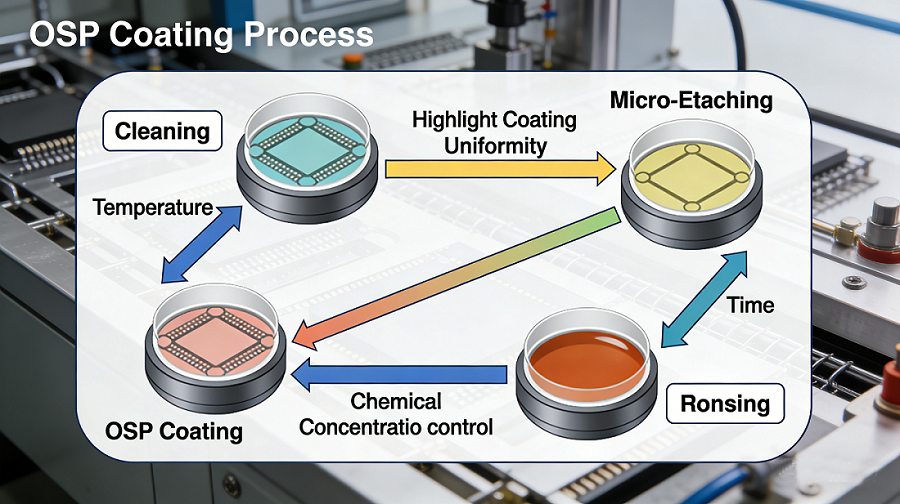
Organic Solderability Preservative, commonly known as OSP, has become a cornerstone suRFace finish in the printed circuit board (PCB) industry, particularly for fine-pitch applications and lead-free assembly processes. Its popularity stems from its cost-effectiveness, flat profile which is ideal for fine-pitch placement, and its ability to protect the underlying copper from oxidation during storage. However, the OSP process is a delicate chemical equilibrium; it is highly sensitive to variations in surface preparation, chemical concentrations, and processing parameters. One of the most prevalent and vexing issues encountered in OSP lines is uneven film thickness across the surface of the PCB. This inconsistency—where some pads have a film that is too thick and others too thin—directly translates to significant solderability problems, manifesting as dewetting, non-wetting, or tombstoning during the reflow soldering process. Resolving this requires a systematic approach that delves into the chemistry of the copper surface, the mechanics of conveyorized processing, and the nuances of micro-etching.
To understand why uneven film thickness causes solderability failures, it is essential to first grasp the mechanism of OSP protection. OSP is a water-based organic compound, typically based on azoles (such as benzotriazole, imidazoles, or benzimidazoles), which chemisorbs onto the copper surface. Unlike solder masks that cover the copper, OSP forms a monolayer or sub-monolayer barrier that is designed to be displaced by the flux during soldering. The flux must first clean the pad by removing the OSP film and any oxides before the molten solder can wet the copper. If the film is unevenly applied—for instance, if a specific pad has a film thickness significantly exceeding the recommended range (usually between 0.2 and 0.5 micrometers, though this varies by vendor)—the flux may struggle to remove this thicker barrier completely. The result is "OSP entrapment," where pockets of the organic film remain, preventing the solder from adhering to the copper and causing dewetting or "orange peel" textures on the solder joint. Conversely, if a pad has an extremely thin or non-existent OSP layer due to uneven application, that copper is left vulnerable to oxidation during storage or preheat stages, leading to non-wetting defects as the flux cannot remove the thick oxide layer quickly enough.
The root cause of this unevenness is rarely singular; it is usually a complex interplay between the cleanliness of the copper prior to OSP application and the dynamics of the conveyor and chemical tanks. The most critical stage in the OSP process is the pre-treatment, specifically the micro-etching and cleaning steps. Copper surfaces that are not uniformly micro-etched will not bond with the OSP chemistry consistently. Micro-etching creates a micro-roughness or "tooth" that increases surface area and provides active sites for the OSP molecules. If the micro-etch rate is inconsistent—perhaps due to uneven spray pressure in the etching tank or air pockets forming under the PCB as it travels through the horizontal conveyor—the copper surface energy will vary across the board. High surface energy areas will attract more OSP molecules, leading to thicker films, while low surface energy or poorly etched areas will result in thinner films. This is often the primary culprit behind "patchy" OSP coverage.
Another significant factor contributing to uneven thickness is the handling of the PCB within the conveyor system, specifically the formation of laminar flow and "shadowing" effects. In horizontal conveyor lines, PCBs travel through chemical tanks on edge or on carriers. If the conveyor speed is too fast, or the nozzle pressure is insufficient, the chemical solution may not fully penetrate the center of large boards or the inner rows of tightly spaced panels. This creates a "shadow" effect where the solution flows over the top edges but does not refresh properly in the center, leading to chemical depletion and thinner OSP films in those shadowed areas. Furthermore, if the PCBs are not racked or supported correctly, bowing can occur, causing the center of the board to lift away from the chemical spray, exacerbating the thickness variation between the edges and the center.
The impact of these variations on solderability is profound and can be observed through specific defect signatures. During the reflow process, when the flux activates, it must aggressively attack the OSP film. On pads with an excessively thick OSP layer, the flux may become exhausted before it can fully clear the organic barrier. As the solder paste melts, it attempts to wet the copper but is blocked by the remaining OSP residue. This leads to the Solder Bead pulling back, creating a dewetting defect where the copper pad is partially exposed. This not only creates an aesthetic issue but also a reliability nightmare, as the reduced solder-to-copper contact area increases electrical resistance and reduces mechanical strength. In high-speed automated optical inspection (AOI), these defects are often flagged as "insufficient solder" or "solder balls," leading to increased rework costs. On the flip side, pads with insufficient OSP thickness oxidize rapidly. When the board enters the reflow oven, the nitrogen atmosphere and flux are often insufficient to reduce the pre-existing oxides, resulting in non-wetting open circuits.
Solving this problem requires a rigorous troubleshooting protocol that begins with the incoming material and ends with the final rinse. The first step is to verify the micro-etch uniformity. The micro-etchant, typically a sulfuric acid/hydrogen peroxide mixture or a persulfate solution, must be monitored for specific gravity and acidity. Operators should perform a "coupon test" where a copper coupon is processed alongside the production panels. By measuring the weight loss of the coupon, one can calculate the etch rate. If the rate is too low, the surface may be passive; if too high, it may be overly aggressive. More importantly, cross-sections of the etched copper should be examined under a scanning electron microscope (SEM) to ensure that the surface roughness is consistent across the entire panel. If striations or uneven etching patterns are visible, the spray nozzles in the pre-treatment section are likely clogged or misaligned and need immediate attention.
Following the micro-etch, the pickling (acid dip) and water rinsing stages are critical. Any residual etchant or contaminants left on the board will act as a barrier to OSP chemisorption. A common issue is "water breaks"—a phenomenon where water beads up on the copper surface instead of sheeting off uniformly—indicating surface contamination. If a water break test fails, it means that organic contaminants (like oils from finger prints or machining fluids) are present. These contaminants will prevent the OSP from bonding, creating thin spots. Therefore, ensuring a perfectly clean surface through multi-stage counter-flow rinsing is non-negotiable.
Once the surface preparation is confirmed to be uniform, the focus shifts to the OSP application tank itself. The concentration of the OSP chemical must be maintained within the vendor's recommended range. If the concentration is too high, the film will deposit too quickly and unevenly; if too low, the film will be thin. The temperature of the OSP tank is equally important. OSP chemistry is temperature-sensitive; higher temperatures generally accelerate the deposition rate. If the tank has hot spots or the heat exchanger is malfunctioning, the film thickness will vary across the board. Agitation within the tank is another key variable. Stagnant OSP solution leads to the depletion of active ingredients in the boundary layer immediately adjacent to the copper. Implementing ultrasonic agitation or ensuring high-turbulence spray nozzles can help refresh this boundary layer, ensuring that every square millimeter of the PCB is exposed to fresh, active chemistry simultaneously.
The conveyor speed, or "dwell time," dictates how long the copper is submerged in the OSP solution. This is a critical parameter that must be optimized based on the specific gravity and temperature of the bath. A speed that is too fast will result in an incomplete monolayer, leading to thin films and oxidation. A speed that is too slow allows for excessive polymerization of the OSP molecules, leading to a thick, tough film that is difficult for the flux to remove. It is often necessary to perform a "thickness profile map" of a test board using an X-ray fluorescence (XRF) spectrometer or a colorimetric thickness tester. By mapping the thickness at multiple points (center, corners, edges), one can identify specific patterns—such as "dog bones" (thick at edges, thin in the middle) or "smile lines"—that correspond to specific equipment issues like uneven spray or racking problems.
The post-OSP rinsing and drying process is the final frontier in preventing unevenness. If the rinse water pressure is too high, it can physically strip the freshly applied, still-wet OSP film from the edges of the pads, creating a "thinning" effect. If the dryer is not functioning correctly, water spots can form. These water spots can cause the OSP film to hydrolyze or wash away, leading to oxidation in those specific areas. A clean, hot-air knife or an infrared dryer with uniform heat distribution is necessary to ensure the film sets properly without any physical distortion.
In conclusion, resolving OSP film thickness unevenness is a holistic exercise in process control. It is not merely about adjusting a single knob on the machine but about understanding the entire ecosystem of the PCB surface finish line. By ensuring uniform micro-roughness through proper pre-treatment, maintaining chemical stability and agitation in the OSP tank, and optimizing conveyor dynamics to prevent shadowing and stagnation, manufacturers can achieve the consistent, defect-free film thickness required for robust solderability. The cost of ignoring these details is high—manifesting in field failures, warranty claims, and damaged reputations. Therefore, a proactive approach to OSP process management, utilizing tools like XRF mapping and strict adherence to water break tests, is the only viable solution to this persistent manufacturing challenge.
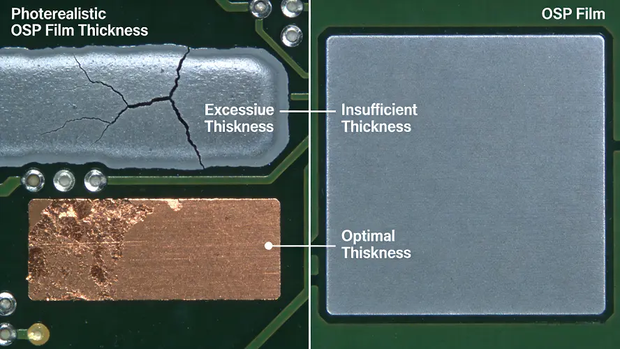
Illustration 1: Mechanism of OSP Film Formation and Failure
This diagram illustrates the molecular interaction between the OSP chemistry and the copper pad, contrasting a healthy application with an uneven one.
- Left Side (Proper Application): Shows a uniform monolayer of OSP molecules (depicted as green chains) chemisorbed onto a uniformly micro-etched copper surface (orange peaks). The flux (blue liquid) is shown easily displacing this layer, allowing molten solder (grey) to wet the copper completely.
- Right Side (Uneven Application): Depicts two scenarios.
- Top: A thick, polymerized OSP layer (dense green mass) where flux has failed to penetrate, resulting in dewetting and solder beading up.
- Bottom: A thin or missing OSP layer due to contamination (black specks), showing oxidation (red rust) forming underneath, preventing any solder adhesion.
- Annotations:
Uniform Micro-EtchOSP MonolayerFlux DisplacementThick OSP Layer (Dewetting)Oxidation due to Thin OSP (Non-wetting)
Illustration 2: Conveyor Shadowing and Chemical Flow Dynamics
This cross-sectional view of a horizontal OSP line explains how physical handling affects chemical coverage.
- Visual: A conveyor belt moving PCBs through a chemical tank.
- Problem Area: The diagram highlights a "shadow zone" in the center of the PCB panel. Arrows representing chemical spray nozzles show the fluid dynamics; the spray hits the edges directly but deflects or stagnates in the center.
- Result: A color gradient overlay on the PCB shows the edges as dark green (thick OSP) and the center as pale yellow (thin OSP).
- Annotations:
Conveyor Finger / CarrierSpray NozzleFluid DeflectionStagnant Boundary Layer (Shadow Zone)Result: Thin Film in Center
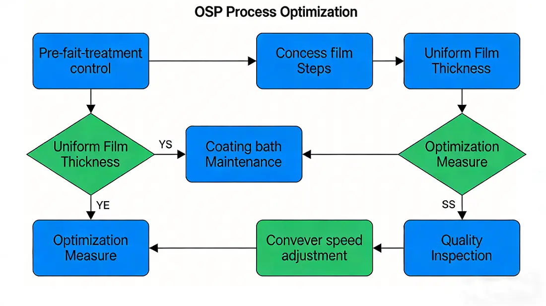
Illustration 3: Process Optimization Workflow for Uniformity
A flowchart-style diagram outlining the steps to diagnose and fix the issue.
- Start:
Solderability Defects Observed. - Step 1:
Micro-Etch Analysis(Check weight loss & surface roughness via SEM). - Step 2:
Water Break Test(Ensure no surface contamination). - Step 3:
OSP Tank Profiling(Check concentration, temperature, and agitation). - Step 4:
XRF Thickness Mapping(Identify pattern of unevenness: Edge vs. Center). - Step 5:
Adjust Conveyor Speed & Nozzles(Optimize dwell time and flow). - End:
Uniform Film Achieved. - Annotations:
Troubleshooting PathCritical Control PointsRoot Cause IdentificationOptimization Parameters