 PCB
PCB FPC
FPC Rigid-Flex
 FR-4
FR-4 HDI PCB
 Rogers High-Frequency Board
 PTFE Teflon High-Frequency Board
 Aluminum
 Copper Core
 PCB Assembly
 LED light PCBA
 Memory PCBA
 Power Supply PCBA
 New Energey PCBA
 Communication PCBA
 Industrial Control PCBA
 Medical Equipment PCBA
 Testing Service
 PCBA Testing Service
 Certification Application
 RoHS Certification Application
 REACH Certification Application
 CE Certification Application
 FCC Certification Application
 CQC Certification Application
 UL Certification Application
 Transformers, Inductors
 High Frequency Transformers
 Low Frequency Transformers
 High Power Transformers
 Conversion Transformers
 Sealed Transformers
 Ring Transformers
 Inductors
 Wires,Cables Customized
 Network Cables
 Power Cords
 Antenna Cables
 Coaxial Cables
 Net Position Indicator
 Solar AIS net position indicator
 Capacitors
 Connectors
 Diodes
 Embedded Processors & Controllers
 Digital Signal Processors (DSP/DSC)
 Microcontrollers (MCU/MPU/SOC)
 Programmable Logic Device(CPLD/FPGA)
 Communication Modules/IoT
 Resistors
 Through Hole Resistors
 Resistor Networks, Arrays
 Potentiometers,Variable Resistors
 Aluminum Case,Porcelain Tube Resistance
 Current Sense Resistors,Shunt Resistors
 Switches
 Transistors
 Power Modules
 Isolated Power Modules
 AC-DC Power Modules
 DC-AC Module(Inverter)
 RF and Wireless
Optimizing High-Frequency Loop Area & Thermal Path in SMPS Layout
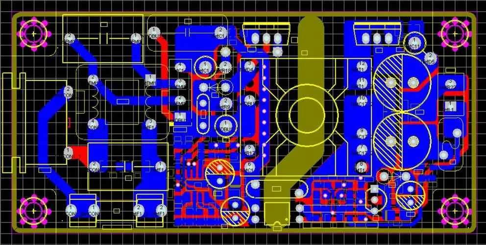
In high-frequency SMPS (>100kHz), loop area and thermal path directly impact EMI and efficiency. Every 1cm² loop area increase rAISes radiation by 6dBμV; 10mΩ thermal path impedance drop reduces efficiency by 0.8%. This guide details optimization through circuit modeling, layout strategies, and empirical data.
1. Critical Loop Analysis
1.1 Three Noise Loops (Fig.1)
| Loop Type | Current Path | Noise Spectrum |
|---|---|---|
| Primary Switching | Cin→Q1→T1→Cin | 10-30MHz |
| Secondary Rectifying | T2→D1→Cout→T2 | 30-100MHz |
| Gate Drive | Driver→Q1_gate→Q1_source | >100MHz |
1.2 Loop Area Model
Radiation intensity:
Where:
-
: Switching freq (MHz)
-
: Peak current (A)
-
: Loop area (cm²)
Target: A<2cm² (300kHz apps)
2. Layout Optimization
2.1 Primary Side (Fig.2a)
-
Placement:
-
Cin to Q1 distance <5mm
-
Direct copper connection from T1 primary to Q1 drain
-
-
Routing:
-
Kelvin connection for gate drive (trace width≥15mil)
-
Switch node copper area ≤20mm²
-
2.2 Secondary Side (Fig.2b)
| Parameter | Baseline | Optimized |
|---|---|---|
| D1 to Cout distance | 12mm | 3mm |
| Loop area | 4.5cm² | 0.8cm² |
| Radiated noise@30MHz | 45dBμV | 32dBμV |
2.3 Thermal Path Design
-
Heat flow:
-
Thermal vias under Q1/D1 (0.3mm dia, 1mm pitch)
-
3oz copper to heatsink
-
-
Thermal resistance:
Optimized junction-case Rth<1.5℃/W (TO-220 example)
3. Stackup & Materials
3.1 4-Layer Stackup
| Layer | Thickness | Function | Key Feature |
|---|---|---|---|
| Top | 2oz Cu | Power routing | Low-Z path |
| Mid1 | 1oz Cu | Solid ground plane | Flux cancellation |
| Mid2 | 1oz Cu | Split power plane | Local islands |
| Bottom | 2oz Cu | Thermal pad | Integrated cooling |
3.2 HF Material Properties
| Property | FR-4 | Rogers 4350B | Application |
|---|---|---|---|
| Dk@1MHz | 4.5 | 3.66 | >500kHz designs |
| Df | 0.02 | 0.004 | Rectifier loops |
| Thermal Conductivity | 0.3 W/mK | 0.6 W/mK | High-power areas |
4. EMI & Thermal Validation
4.1 Test Data (500W LLC Converter)
| Metric | Baseline | Optimized | Improvement |
|---|---|---|---|
| Conducted EMI@150kHz | 65dBμV | 52dBμV | -13dB |
| Radiated peak@89MHz | 48dBμV/m | 36dBμV/m | -12dB |
| Efficiency@230VAC | 92.3% | 94.1% | +1.8% |
| MOSFET ΔT | 78℃ | 61℃ | -17℃ |
4.2 Thermal Imaging (Fig.3)
-
Hotspot distribution:
-
Baseline: MOSFET center 125℃ (ΔT=35℃)
-
Optimized: Max 108℃ (ΔT<15℃)
-
5. Special Case Solutions
5.1 Multi-Phase Converters
-
Symmetrical layout: <15% loop area variation
-
Phase interleaving: 180°/n phase shift to cancel di/dt noise
5.2 Ultra-Thin Designs
-
Vertical stacking:
-
Power layer adjacent to ground (≤0.2mm spacing)
-
Planar magnetics (<3mm height)
-
-
Nanocrystalline CM chokes: 60% smaller than ferrite