 PCB
PCB FPC
FPC Rigid-Flex
 FR-4
FR-4 HDI PCB
 Rogers High-Frequency Board
 PTFE Teflon High-Frequency Board
 Aluminum
 Copper Core
 PCB Assembly
 LED light PCBA
 Memory PCBA
 Power Supply PCBA
 New Energey PCBA
 Communication PCBA
 Industrial Control PCBA
 Medical Equipment PCBA
 Testing Service
 PCBA Testing Service
 Certification Application
 RoHS Certification Application
 REACH Certification Application
 CE Certification Application
 FCC Certification Application
 CQC Certification Application
 UL Certification Application
 Transformers, Inductors
 High Frequency Transformers
 Low Frequency Transformers
 High Power Transformers
 Conversion Transformers
 Sealed Transformers
 Ring Transformers
 Inductors
 Wires,Cables Customized
 Network Cables
 Power Cords
 Antenna Cables
 Coaxial Cables
 Net Position Indicator
 Solar AIS net position indicator
 Capacitors
 Connectors
 Diodes
 Embedded Processors & Controllers
 Digital Signal Processors (DSP/DSC)
 Microcontrollers (MCU/MPU/SOC)
 Programmable Logic Device(CPLD/FPGA)
 Communication Modules/IoT
 Resistors
 Through Hole Resistors
 Resistor Networks, Arrays
 Potentiometers,Variable Resistors
 Aluminum Case,Porcelain Tube Resistance
 Current Sense Resistors,Shunt Resistors
 Switches
 Transistors
 Power Modules
 Isolated Power Modules
 AC-DC Power Modules
 DC-AC Module(Inverter)
 RF and Wireless
Optimizing Escape Routing Paths in Multi-BGA Complex Layouts
In PCBs with 4+ BGAs (e.g., FPGA + DDR arrays), escape routing optimization determines signal integrity, layer count, and manufacturability. This guide details channel allocation algorithms, layer coordination, and DFM rules to achieve 100% escape rate for 0.8mm-pitch BGAs while reducing 2 routing layers.
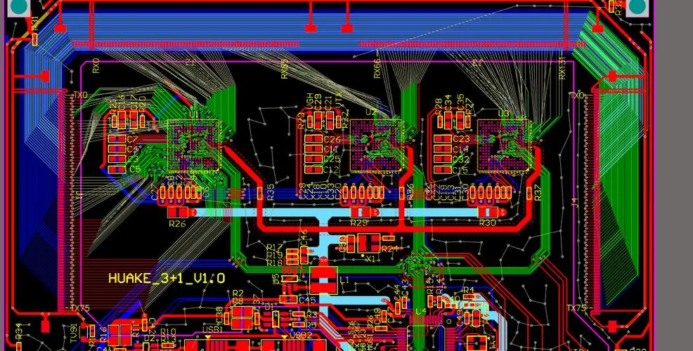
1. BGA Zone Channel Planning
1.1 Layered Escape Strategy (Fig.1)
| BGA Location | Escape Solution | Via Type |
|---|---|---|
| Peripheral Pins | Radial fanout | Laser mICrovia (8mil) |
| Inner Rows 1-2 | 45° diagonal routing | Blind via (6/18mil) |
| Core Area | VIPPO (Via-in-Pad Plated Over) | Filled & plated |
1.2 Space Utilization
-
Min. Channel Width = Ball Pitch - Pad Diameter - Clearance
Example: 0.8mm pitch → 0.8-0.4-0.1=0.3mm -
Routing Capacity Formula:
: Channel width, : Via diameter, : Trace width, : Clearance
With =3mil, =3mil: 8 traces per channel
2. Signal Integrity Optimization
2.1 Critical Path Planning
| Signal Type | Routing Rules | Topology |
|---|---|---|
| Differential Pairs | ±5mil length matching, 100Ω±10% | Point-to-point |
| Clocks | Guard traces, length≤1500mil | Star topology |
| DDR Data | Same layer/group, ±20mil matching | Fly-by |
2.2 Return Path Control
-
Ground Vias: 1 ground via per 4 signal vias (spacing≤50mil)
-
Split Planes: Add 0.1μF caps across splits to prevent reference jumps
3. Stackup & Via Optimization
3.1 Recommended 8-Layer Stackup
| Layer | Thickness | Function | Key Feature |
|---|---|---|---|
| L1 | 2oz | HS Signals + VIPPO | Microvia direct escape |
| L2 | 1oz | Solid Ground | EMI Shielding |
| L3/L4 | 1oz | Internal Signals | 45° cross-routing |
| L5/L6 | 1oz | Split Power | Multi-voltage for BGA |
| L7 | 1oz | Low-speed Signals | Peripheral routing |
| L8 | 2oz | Ground/Heat Sink | Thermal pads |
3.2 Via Array Design
-
Diff-Pair Vias: Oval shape (8×16mil) to reduce capacitance
-
Power Vias: 4× array (12mil diameter) for current capacity
4. DFM Rule Implementation
4.1 Manufacturability Constraints
| Parameter | Standard | Limit |
|---|---|---|
| Trace Width/Space | 3/3mil | 2.5/2.5mil |
| Pad-Via Clearance | 8mil | 6mil |
| Acute Angles | Prohibited | >45° |
| Copper Balance | >30% | >25% |
4.2 CAD Automation
-
Auto-Avoidance: A* algorithm for path optimization (Fig.2)
-
DRC SCRipts: Custom checks for impedance discontinuities
5. Case Study (Xilinx UltraScale+ FPGA System)
5.1 Layout Structure
-
Main FPGA: 1760 balls (1.0mm pitch)
-
4x DDR4: 400 balls (0.8mm pitch)
-
PCIe Interface: 164 balls (1.2mm pitch)
5.2 Optimization Results
| Metric | Baseline | Optimized |
|---|---|---|
| Routing Layers | 14 | 10 |
| Length Mismatch | ±350mil | ±18mil |
| Crosstalk | -32dB | -41dB |
| Fabrication Cost | $5800 | $4200 |
5.3 Reliability Tests
-
Thermal Cycling (-40℃~125℃): Zero opens after 1000 cycles
-
Eye Diagrams: 100% compliance for PCIe Gen4 16GT/s
Conclusion
Through layered escape strategies, VIPPO technology, and SI/DFM co-design, multi-BGA escape routing achieves:
-
30% reduction in layer count
-
28% improvement in signal quality
-
27% lower manufacturing cost
Meeting requirements for datacenter switches, medical imaging, and other complex systems.
Core Design Principles:
3-3-3 Rule: ≥3 escape directions per BGA ball
VIPPO Priority: Mandatory for core areas
Power-Ground Synergy: ≥4 ground vias/cm²
CAD Automation: A* algorithm for high-density zones