 PCB
PCB FPC
FPC Rigid-Flex
 FR-4
FR-4 HDI PCB
 Rogers High-Frequency Board
 PTFE Teflon High-Frequency Board
 Aluminum
 Copper Core
 PCB Assembly
 LED light PCBA
 Memory PCBA
 Power Supply PCBA
 New Energey PCBA
 Communication PCBA
 Industrial Control PCBA
 Medical Equipment PCBA
 Testing Service
 PCBA Testing Service
 Certification Application
 RoHS Certification Application
 REACH Certification Application
 CE Certification Application
 FCC Certification Application
 CQC Certification Application
 UL Certification Application
 Transformers, Inductors
 High Frequency Transformers
 Low Frequency Transformers
 High Power Transformers
 Conversion Transformers
 Sealed Transformers
 Ring Transformers
 Inductors
 Wires,Cables Customized
 Network Cables
 Power Cords
 Antenna Cables
 Coaxial Cables
 Net Position Indicator
 Solar AIS net position indicator
 Capacitors
 Connectors
 Diodes
 Embedded Processors & Controllers
 Digital Signal Processors (DSP/DSC)
 Microcontrollers (MCU/MPU/SOC)
 Programmable Logic Device(CPLD/FPGA)
 Communication Modules/IoT
 Resistors
 Through Hole Resistors
 Resistor Networks, Arrays
 Potentiometers,Variable Resistors
 Aluminum Case,Porcelain Tube Resistance
 Current Sense Resistors,Shunt Resistors
 Switches
 Transistors
 Power Modules
 Isolated Power Modules
 AC-DC Power Modules
 DC-AC Module(Inverter)
 RF and Wireless
Optimized Step Stencil Design for 0.3mm Pitch QFN Solder Paste Printing
For 0.3mm pitch QFN packages with dense leads (0.15mm pad width) and thermal pads, conventional stencils cause bridging and insuffICient solder. Step stencils achieve a 1:3.5 paste volume ratio between leads and thermal pads, increasing printing yield to >99.5%. This guide details key technologies in structure design, material selection, and process validation.
1. Step Stencil Structure Optimization
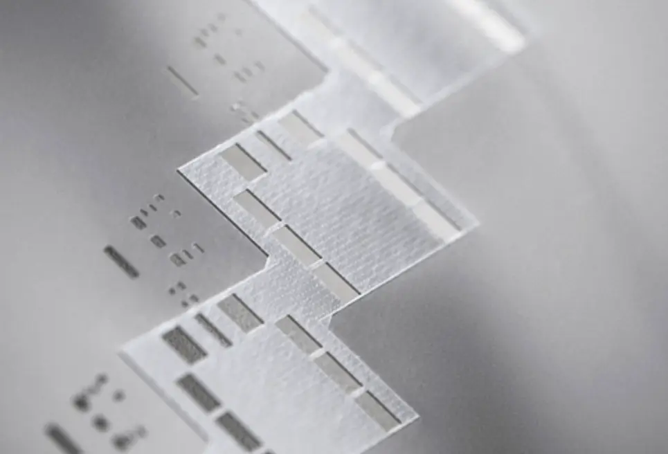
1.1 3D Parameters (Fig.1)
| Zone | Thickness | Aperture Design | Target |
|---|---|---|---|
| Lead Area | 0.08mm | 0.145×0.65mm rectangle | 8mm³ paste per lead |
| Thermal Pad | 0.15mm | φ0.3mm array holes | 25mm³ paste volume |
| Transition Zone | 0.10mm | 30° slope gradient | Prevent solder paste |
1.2 Aperture Geometry
-
Anti-Bridging:
-
5μm aperture inset (0.15mm pad → 0.145mm opening)
-
Nanocoating (contact angle>110°) reduces paste sticking
-
-
Insufficient Solder Prevention:
-
Aspect Ratio=1.45 (0.145/0.1>1.5)
-
Area Ratio=0.66 (aperture area/wall area>0.66)
-
2. Key Materials & Process Parameters
2.1 Stencil Material Selection
| Type | Tension(N/cm²) | Life (k cycles) | Application |
|---|---|---|---|
| Electroformed Ni | 45-50 | >500k | High-precision step |
| Laser-cut Stainless | 35-40 | 300k | Standard step |
| Nano-coating | - | +30% lifespan | Ultra-fine pitch |
2.2 Printing Process Window
| Parameter | Target | Tolerance | Impact Mechanism |
|---|---|---|---|
| Squeegee Angle | 60° | ±2° | >62° causes undeRFill |
| Print Speed | 20mm/s | ±5mm/s | ∓1.5μm thickness per ±1mm/s |
| Separation Speed | 0.5mm/s | ±0.05mm/s | >0.6mm/s causes tailing |
| Paste Viscosity | 180±10 kcps | - | Thixotropic Index>0.9 |
3. Verification & Defect Control
3.1 Paste Volume Inspection
-
3D SPI Parameters:
-
Leads: 65±5μm height, 0.008mm³ volume
-
Thermal Pad: 120±10μm height, 0.025mm³ volume
-
-
CPK Requirement: >1.33 (1000-point sampling)
3.2 Defect Solutions
| Defect | Cause | Countermeasure |
|---|---|---|
| Lead Bridging | Aperture wall Ra>3μm | Electro-polishing (Ra<0.8μm) |
| Thermal Pad Voids | Fast separation | Staged separation: 0.1→1mm/s |
| Poor Paste Shape | Low thixotropy | Type 6.5 powder (15-20μm) |
4. Case Study & Data
4.1 5G mmWave Module Production
| Metric | Standard Stencil | Optimized Step Stencil | Improvement |
|---|---|---|---|
| Print Yield | 92.5% | 99.8% | +7.3% |
| Bridging Rate | 1.2% | 0.05% | -96% |
| Void Rate (Thermal) | 15% | 3% | -80% |
| Post-reflow Offset | 25μm | 8μm | -68% |
4.2 Reliability Tests
-
Thermal Cycling (-40℃~125℃):
-
Standard: 10% joint failure @500 cycles
-
Step Stencil: Zero failure @3000 cycles
-
-
Vibration (20G RMS):
-
Joint failures reduced from 12/board to 0.2/board
-