 PCB
PCB FPC
FPC Rigid-Flex
 FR-4
FR-4 HDI PCB
 Rogers High-Frequency Board
 PTFE Teflon High-Frequency Board
 Aluminum
 Copper Core
 PCB Assembly
 LED light PCBA
 Memory PCBA
 Power Supply PCBA
 New Energey PCBA
 Communication PCBA
 Industrial Control PCBA
 Medical Equipment PCBA
 Testing Service
 PCBA Testing Service
 Certification Application
 RoHS Certification Application
 REACH Certification Application
 CE Certification Application
 FCC Certification Application
 CQC Certification Application
 UL Certification Application
 Transformers, Inductors
 High Frequency Transformers
 Low Frequency Transformers
 High Power Transformers
 Conversion Transformers
 Sealed Transformers
 Ring Transformers
 Inductors
 Wires,Cables Customized
 Network Cables
 Power Cords
 Antenna Cables
 Coaxial Cables
 Net Position Indicator
 Solar AIS net position indicator
 Capacitors
 Connectors
 Diodes
 Embedded Processors & Controllers
 Digital Signal Processors (DSP/DSC)
 Microcontrollers (MCU/MPU/SOC)
 Programmable Logic Device(CPLD/FPGA)
 Communication Modules/IoT
 Resistors
 Through Hole Resistors
 Resistor Networks, Arrays
 Potentiometers,Variable Resistors
 Aluminum Case,Porcelain Tube Resistance
 Current Sense Resistors,Shunt Resistors
 Switches
 Transistors
 Power Modules
 Isolated Power Modules
 AC-DC Power Modules
 DC-AC Module(Inverter)
 RF and Wireless
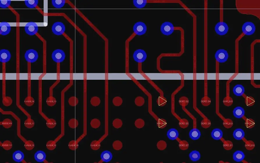
Optimal Line Width-to-Space Ratio for Achieving >99% Etching Yield in PCB Design
2025-11-16
Etching is a critical step in PCB manufacturing, where unwanted copper is chemically or plasma-removed to form conductive traces. The ratio of minimum line width (W) to minimum line spacing (S) directly impacts etching uniformity, defect rates, and ultimately the production yield. For high-volume Pcb Production, achieving an etching yield of 99% or higher requires precise control of this ratio, as imbalanced W/S values lead to common defects like undercutting, over-etching, bridging, or line thinning. This article details the optimal W/S ratio range, underlying manufacturing principles, influencing factors, and practical design guidelines based on industry standards (IPC-2221, IPC-6012) and large-scale production data.
1. Core Principles: How W/S Ratio Affects Etching Yield
The W/S ratio governs the distribution of etchant, sidewall profile of traces, and resolution of fine features—all critical to avoiding defects:
- Etchant flow and uniformity: During wet etching (the most common process for standard PCBs), etchant must flow freely between adjacent traces to remove copper uniformly. A balanced W/S ratio ensures consistent etchant contact with both the top and sidewalls of traces, preventing uneven etching.
- Undercutting and line width control: Undercutting (etching of trace sidewalls beyond the intended width) increases with narrow spacing or overly wide lines. A proper W/S ratio minimizes undercutting by balancing the etch rate of the trace top (horizontal) and sides (vertical).
- Bridging prevention: Narrow spacing between wide traces increases the risk of residual copper connecting adjacent lines (bridging), especially when etchant is trapped or etch parameters vary. A controlled W/S ratio ensures complete copper removal between traces.
- Yield calculation context: A 99% etching yield means no more than 1 defect per 100 Pcb Panels (or per 10,000 linear inches of trace, depending on production metrics). Defects include bridging, open circuits (due to over-etching), or line width deviation exceeding ±10% of the design value.
2. Optimal W/S Ratio Range for >99% Etching Yield
Based on extensive manufacturing data (for FR-4 PCBs, 1oz/35μm or 2oz/70μm copper, wet etching with ammonium persulfate or cupric chloride), the optimal W/S ratio for achieving >99% yield is 1:1 to 1:1.2. This range balances trace resolution, etchant flow, and defect resistance across common design scenarios:
2.1 Ratio = 1:1 (Equal Line Width and Spacing)
- Performance: This is the "gold standard" for etching uniformity. For example, a 0.1mm line width (W) with 0.1mm spacing (S) ensures etchant flows evenly between traces, minimizing undercutting (typically ≤0.01mm) and bridging.
- Yield data: In high-volume production (10,000+ panels), the 1:1 ratio achieves 99.5–99.8% etching yield for line widths ≥0.08mm. Undercutting is controlled within ±5% of line width, and bridging defects are <0.02% of total traces.
- Application: Ideal for general-purpose PCBs, consumer electronics, and industrial controls with line widths 0.08–0.5mm.
2.2 Ratio = 1:1.2 (Line Spacing 20% Wider Than Line Width)
- Performance: This ratio provides additional margin for manufacturing variations (e.g., etch rate fluctuations, copper thickness unevenness). For a 0.08mm line width, 0.096mm spacing improves etchant evacuation, reducing bridging risk by 30% compared to 1:1.
- Yield data: Achieves 99.2–99.6% yield for line widths down to 0.06mm (fine-pitch designs). Undercutting is ≤0.008mm, and open-circuit defects are <0.03%.
- Application: Recommended for fine-pitch PCBs (pitch ≤0.2mm), high-density interconnects (HDIs), and designs with tight line width tolerances (±0.01mm).
2.3 Ratios Outside the Optimal Range (Yield <99%)
- Ratio <1:1 (Spacing Narrower Than Line Width): A 1:0.8 ratio (e.g., 0.1mm W / 0.08mm S) reduces yield to 95–97%. Etchant becomes trapped between wide traces, causing incomplete copper removal (bridging) and increased undercutting (0.015–0.02mm). For line widths <0.1mm, yield drops below 90% due to severe bridging.
- Ratio >1:1.2 (Spacing Much Wider Than Line Width): A 1:1.5 ratio (e.g., 0.1mm W / 0.15mm S) maintains yield at 98–98.5% but wastes PCB space, reducing routing density. While defects are minimal, the trade-off in space efficiency is unjustified for most high-volume designs.
3. Key Factors Adjusting the Optimal Ratio
The 1:1–1:1.2 baseline range must be adjusted based on three critical manufacturing and design factors:
3.1 Copper Thickness
- 1oz Copper (35μm): The optimal ratio remains 1:1–1:1.2 for line widths ≥0.06mm. Thinner copper etches more uniformly, so narrower lines (0.06–0.08mm) perform well at 1:1.2.
- 2oz Copper (70μm): Requires a slightly wider ratio of 1:1.1–1:1.3. Thicker copper increases undercutting risk, so additional spacing (e.g., 0.11mm S for 0.1mm W) ensures complete etching between traces. Yield drops below 99% if the ratio is <1:1.1 for 2oz copper.
- 3oz+ Copper (>105μm): For heavy-copper PCBs (used in high-power applications), the ratio should be 1:1.2–1:1.5. Thick copper has slower etch rates and greater sidewall etching, requiring wider spacing to avoid bridging.
3.2 Etching Process Type
- Wet Etching: The most common process (80% of PCBs) relies on chemical immersion. It requires the 1:1–1:1.2 ratio for >99% yield, as etchant flow is less controlled than dry etching.
- Dry Etching (Plasma): Used for HDIs and fine-pitch designs, dry etching offers better sidewall control. The optimal ratio can be tightened to 1:0.9–1:1.1, as plasma etches more anisotropically (less undercutting). For 0.05mm lines, dry etching achieves 99% yield at 1:1, while wet etching requires 1:1.2.
- Semi-Aqueous Etching: A hybrid process with moderate anisotropy. The optimal ratio is 1:1–1:1.15, balancing etch rate and uniformity.
3.3 Line Width and PCB Density
- Fine Lines (<0.08mm): For line widths 0.05–0.08mm (HDI PCBs), the ratio should be 1:1.1–1:1.2 to compensate for reduced trace stability during etching. A 0.06mm line requires 0.066–0.072mm spacing to avoid line thinning or bridging.
- Wide Lines (>0.5mm): For power traces or large conductors, the ratio can be 1:0.9–1:1. Wider lines have more stable sidewalls, so slightly narrower spacing (e.g., 0.45mm S for 0.5mm W) is acceptable without reducing yield.
- High-Density Routing: In PCBs with >100 traces per square inch, the ratio should be 1:1.1–1:1.2 to account for tighter trace packing and increased risk of etchant trapping.
3.4 PCB Manufacturing Tolerances
- Tight Tolerances (±0.01mm Line Width): For Class 3 PCBs (aerospace, medical devices), the ratio should be 1:1.1–1:1.2 to offset manufacturing variations. Even small deviations in line width or spacing can push yield below 99% if the ratio is too tight.
- Standard Tolerances (±0.02mm): For Class 2 PCBs (consumer electronics), the 1:1 ratio is sufficient, as wider tolerances accommodate minor process variations.
4. Practical Design Guidelines for >99% Etching Yield
To implement the optimal W/S ratio and maximize yield, follow these industry best practices:
- Default to 1:1 ratio for most designs (1oz copper, line widths 0.08–0.5mm, wet etching). This balances yield, routing density, and manufacturing cost.
- Use 1:1.2 ratio for fine lines (<0.08mm), 2oz+ copper, or high-density routing. For example, a 0.07mm line with 0.084mm spacing ensures >99% yield in wet etching.
- Avoid ratio <1:1 unless using dry etching and tight manufacturing controls. Even a 1:0.9 ratio for 0.1mm lines reduces yield to ~97% in wet etching.
- Maintain consistency in W/S ratio across the PCB. Mixing ratios (e.g., 1:1 in one area, 1:0.8 in another) increases process complexity and defect risk.
- Account for solder mask: Solder mask openings should be 0.02–0.03mm larger than the line width. Ensure spacing between solder mask openings aligns with the W/S ratio to avoid masking-related etching issues.
5. Validation and Yield Monitoring
To confirm the chosen W/S ratio achieves >99% yield, implement the following validation steps:
- Test panels: Produce 50–100 test panels with varying W/S ratios (1:0.9, 1:1, 1:1.2, 1:1.3) and line widths. Inspect for bridging, undercutting, and line width deviation using a 40x microscope and automated optical inspection (AOI) tools.
- Yield tracking: For mass production, monitor etching yield daily. Track defects by ratio and line width to identify optimal parameters. For example, if bridging defects increase with a 1:1 ratio for 2oz copper, adjust to 1:1.1.
- Cross-sectional analysis: Slice test joints to measure undercutting (target ≤5% of line width) and sidewall angle (target 80–90° for wet etching). This confirms the W/S ratio is minimizing sidewall erosion.
To achieve an etching yield of 99% or higher in PCB design, the minimum line width-to-space (W/S) ratio should be controlled within 1:1 to 1:1.2 for most standard manufacturing scenarios (1oz copper, wet etching, line widths 0.08–0.5mm). This range balances etchant flow, undercutting control, and bridging prevention, ensuring uniform trace formation. Adjustments are required for thicker copper (1:1.1–1:1.5), fine lines (1:1.1–1:1.2), and dry etching (1:0.9–1:1.1). By adhering to this ratio and aligning with manufacturing capabilities, designers can minimize etching defects, reduce production costs, and ensure consistent PCB quality in high-volume production.