 PCB
PCB FPC
FPC Rigid-Flex
 FR-4
FR-4 HDI PCB
 Rogers High-Frequency Board
 PTFE Teflon High-Frequency Board
 Aluminum
 Copper Core
 PCB Assembly
 LED light PCBA
 Memory PCBA
 Power Supply PCBA
 New Energey PCBA
 Communication PCBA
 Industrial Control PCBA
 Medical Equipment PCBA
 Testing Service
 PCBA Testing Service
 Certification Application
 RoHS Certification Application
 REACH Certification Application
 CE Certification Application
 FCC Certification Application
 CQC Certification Application
 UL Certification Application
 Transformers, Inductors
 High Frequency Transformers
 Low Frequency Transformers
 High Power Transformers
 Conversion Transformers
 Sealed Transformers
 Ring Transformers
 Inductors
 Wires,Cables Customized
 Network Cables
 Power Cords
 Antenna Cables
 Coaxial Cables
 Net Position Indicator
 Solar AIS net position indicator
 Capacitors
 Connectors
 Diodes
 Embedded Processors & Controllers
 Digital Signal Processors (DSP/DSC)
 Microcontrollers (MCU/MPU/SOC)
 Programmable Logic Device(CPLD/FPGA)
 Communication Modules/IoT
 Resistors
 Through Hole Resistors
 Resistor Networks, Arrays
 Potentiometers,Variable Resistors
 Aluminum Case,Porcelain Tube Resistance
 Current Sense Resistors,Shunt Resistors
 Switches
 Transistors
 Power Modules
 Isolated Power Modules
 AC-DC Power Modules
 DC-AC Module(Inverter)
 RF and Wireless
Common Treatment Methods for Post-Etch Circuit Residues (Open-Circuit Risks) in PCB Manufacturing
2025-11-19
Etching is a critical step in Pcb Fabrication that defines conductive traces by removing unwanted copper, but post-etch circuit residues—such as partial copper removal, residual conductive debris, or incomplete trace formation—pose significant open-circuit risks. These residues often stem from uneven etchant distribution, inadequate resist adhesion, copper oxidation, or process parameter deviations, and if left unaddressed, can lead to intermittent connectivity, signal integrity degradation, or complete circuit failure. This article details the common treatment methods for post-etch circuit residues, categorized by residue type and application scenario, while aligning with industry standards such as IPC-7721 and IPC-A-610.
1. Pre-Treatment: Residue Diagnosis and Classification
Effective residue treatment begins with accurate diagnosis to identify residue type, location, and severity—critical for selecting the appropriate repair strategy:
- Residue Types and Open-Circuit Mechanisms:
- Partial Copper Residues: Incomplete etch of copper between traces or on trace edges, leading to potential bridging or localized conductivity loss.
- Conductive Debris: Oxidized copper particles (Cu₂O/CuO) or metallic fragments trapped between traces, causing intermittent short circuits that may evolve into open circuits under thermal cycling.
- Resist Residues: Remnants of photoresist or solder mask that block copper etching, resulting in thin, weak traces prone to cracking (micro-open-circuit risks).
- Etchant Residues: Chemical byproducts (e.g., cupric chloride salts) that corrode copper over time, creating etch pits and eventual trace breakage.
- Diagnostic Tools:
- Automated Optical Inspection (AOI): Detects suRFace residues and trace irregularities with 5–10μm precision, ideal for high-volume production.
- X-Ray Inspection: Identifies hidden residues in multi-layer PCBs (MLBs) or HDIs, such as inner-layer copper fragments or partial etch defects.
- Electrical Testing: Uses multimeters (continuity checks) or Time-Domain Reflectometers (TDR) for high-frequency lines to locate resistance anomalies (>10Ω indicates potential open-circuit risks).
- Microscopic Inspection: 50–200x stereo microscopes verify residue morphology and trace integrity, distinguishing between conductive and non-conductive residues.
2. Core Treatment Methods for Post-Etch Residues
2.1 Chemical Cleaning: Removing Non-Conductive and Light Conductive Residues
Chemical cleaning is the primary method for bulk residue removal, targeting resist remnants, etchant salts, and light oxidation:
- Descumming and Resist Stripping:
- Process: Immerse PCBs in alkaline stripping solutions (e.g., 5–10% sodium hydroxide) at 40–60°C for 5–10 minutes to dissolve photoresist residues. For stubborn resist, add 1–2% surfactant to enhance penetration.
- Post-Cleaning: Rinse thoroughly with deionized water (DI water) to remove chemical residues, then dry with hot air (60–80°C) to prevent moisture-induced corrosion.
- Etchant Residue Removal:
- Use acidic neutralization solutions (e.g., 5% citric acid or 3% hydrochloric acid) to dissolve cupric chloride or ammonium persulfate residues. Soak time is limited to 2–3 minutes to avoid over-etching copper.
- For HDIs, employ spray cleaning (pressure: 0.2–0.3MPa) to reach narrow trace gaps (≤0.1mm), ensuring complete residue evacuation.
- Light Oxidation Removal:
- Apply dilute phosphoric acid (3–5%) at room temperature for 30–60 seconds to remove thin copper oxide layers, followed by DI water rinsing and immediate drying. This preserves trace thickness while restoring conductivity.
2.2 Mechanical Treatment: Eliminating Stubborn Conductive Residues
Mechanical methods target solid conductive residues (e.g., copper fragments, thick oxidation) that resist chemical cleaning:
- Precision Scraping:
- Use ultra-fine tools (tungsten carbide scrapers, 0.05mm diameter needles) to manually remove residues between traces. Operate under a microscope to avoid scratching trace surfaces or damaging adjacent conductors.
- For fine-pitch traces (pitch ≤0.15mm), use ultrasonic cleaning pens (40kHz frequency, ≤5W power) to dislodge trapped debris without mechanical contact.
- Micro-Abrasion:
- Employ 4000–6000 grit wet sandpaper or cerium oxide polishing pads to gently abrade thick residue layers. Use DI water as a lubricant to minimize trace thinning (abrasion depth ≤1μm).
- For localized residues, apply abrasive pastes (alumina particle size: 1–3μm) with a soft brush, followed by thorough cleaning to remove abrasive particles.
- Laser Ablation:
- Ideal for high-precision applications (e.g., 5G PCBs, automotive ECUs) and inner-layer residues. Use 355nm ultraviolet lasers or 1064nm fiber lasers with 20–50μm spot diameters to selectively vaporize conductive residues.
- Key parameters: Power 5–10W, pulse duration 10–20ms, thermal affected zone (HAZ) <20μm to avoid damaging PCB substrates (e.g., FR-4) or adjacent traces.
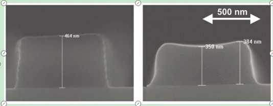
2.3 Trace Repair: Addressing Partial Etch and Micro-Open-Circuit Risks
When residues cause partial trace thinning or incipient breaks, targeted repair restores structural and electrical integrity:
- Wire Bonding (Jumper Repair):
- Application: Suitable for surface traces and accessible inner layers. Use oxygen-free copper wires (diameter 0.08–0.1mm) matching trace width (e.g., 0.1mm wire for 0.15mm traces).
- Process: Clean trace endpoints with anhydrous ethanol, solder wires to endpoints using a 320±10°C soldering iron (welding time ≤3 seconds per joint), and insulate with epoxy-based conformal coating (thickness 20–30μm) to prevent short circuits.
- Reliability: Ensures mechanical strength (pull force ≥50g) and low resistance (≤0.1Ω), compliant with IPC-7721 standards.
- Conductive Paste/Ink Repair:
- Application: Ideal for fine-pitch traces (≤0.1mm), dense component areas, or heat-sensitive PCBs (e.g., flex PCBs).
- Material Selection: Silver-based conductive pastes (volume resistivity ≤1×10⁻⁴Ω·cm) or copper-filled conductive inks, cured at 80–120°C for 30–60 minutes (low-temperature curing avoids component damage).
- Process: Apply paste using 0.1mm diameter syringes to match trace width, ensuring no overflow (to prevent bridging). Post-curing, test conductivity and inspect for adhesion.
- Laser Cladding and Electroplating:
- Application: High-reliability PCBs (aerospace, medical devices) with ultra-fine traces or deep inner-layer defects.
- Process: Use femtosecond laser to melt nano-copper powder onto thinned traces, forming a 1.5–3μm thick conductive layer. Follow with chemical mechanical polishing (CMP) to smooth surfaces (Ra ≤3nm) and chemical copper plating for uniform thickness.
- Advantage: Repairs traces as narrow as 0.05mm and lengths up to 15mm, with impedance deviation ≤±2% for high-frequency signals.
2.4 Rework for Severe Defects
For PCBs with extensive residue-induced damage (e.g., multiple trace breaks, widespread bridging), rework processes restore functionality:
- Selective Etching:
- Apply photoresist to mask intact traces, then use low-concentration etchant (10% sulfuric acid + 5% hydrogen peroxide with 0.1% inhibitor) to remove excessive copper residues. This targets only defective areas, minimizing material loss.
- Resist Reapplication and Re-Etching:
- Strip all remaining resist, clean the PCB thoroughly, reapply photoresist, and re-etch the affected area. This is suitable for PCBs with incomplete trace formation due to initial resist misalignment or residue contamination.
- Component Relocation:
- For residue damage in component pads, relocate non-critical components to undamaged areas and reroute traces using jumper wires or conductive paste. This avoids scrapping entire PCBs for localized defects.
3. Post-Treatment Validation and Quality Control
To ensure residue removal and repair effectiveness, implement the following validation steps:
- Visual and Microscopic Inspection: Confirm no residual debris, trace damage, or repair material overflow using AOI and 200x microscopes.
- Electrical Testing:
- Continuity testing: Ensure repaired traces have resistance ≤0.1Ω (consistent with intact traces).
- Insulation resistance testing: Verify ≥10¹¹Ω between adjacent traces to rule out hidden bridging.
- High-frequency testing: Use Vector Network Analyzers (VNA) for GHz-range traces to confirm impedance deviation ≤±1% and insertion loss increase ≤0.1dB/m.
- Environmental and Mechanical Reliability Testing:
- Thermal cycling: Subject PCBs to 1000–2000 cycles (-40°C to 125°C) to ensure repairs withstand thermal stress without cracking.
- Corrosion resistance: Expose PCBs to 85°C/85% RH for 500 hours (accelerated aging) to confirm no post-repair oxidation.
4. Prevention: Minimizing Post-Etch Residues at the Source
While effective treatment methods exist, prevention is key to reducing open-circuit risks:
- Pre-Etch Preparation: Ensure PCB surfaces are clean (free of oil, fingerprints, and dust) and photoresist adhesion is uniform (pre-bake at 90–100°C for 30 minutes).
- Etching Process Optimization: Maintain etchant concentration (e.g., 180–220g/L for cupric chloride) and temperature (45–55°C) within tight tolerances, and ensure uniform spray pressure (0.25–0.3MPa).
- Post-Etch Cleaning Protocol: Implement a three-step cleaning process—rinse with DI water, neutralize with acidic/alkaline solutions, and dry with filtered hot air—to remove all etchant and resist residues promptly.
5. Compliance with Industry Standards
All residue treatment and repair processes must adhere to IPC standards:
- IPC-7721: Governs PCB repair procedures, requiring repair documentation, material compatibility, and reliability testing.
- IPC-A-610: Specifies acceptability criteria for repaired traces, including maximum repair length (≤15mm for Class 3 applications) and insulation requirements.
- IPC-J-STD-001: Mandates solder quality for jumper repairs, including solder joint fillet shape and wetting.
Post-etch circuit residues pose significant open-circuit risks, but targeted treatment methods—ranging from chemical cleaning and mechanical removal to precision trace repair and rework—effectively mitigate these issues. The choice of method depends on residue type, trace size, PCB complexity, and application reliability requirements: chemical cleaning for bulk residues, laser ablation for high-precision removal, jumper wires or conductive paste for surface trace repairs, and laser cladding for critical inner-layer defects. By combining proper diagnosis, standardized treatment, rigorous validation, and proactive prevention, manufacturers can achieve >99% yield and ensure long-term PCB reliability, even in demanding applications like automotive electronics, aerospace systems, and high-frequency communication devices.