 PCB
PCB FPC
FPC Rigid-Flex
 FR-4
FR-4 HDI PCB
 Rogers High-Frequency Board
 PTFE Teflon High-Frequency Board
 Aluminum
 Copper Core
 PCB Assembly
 LED light PCBA
 Memory PCBA
 Power Supply PCBA
 New Energey PCBA
 Communication PCBA
 Industrial Control PCBA
 Medical Equipment PCBA
 Testing Service
 PCBA Testing Service
 Certification Application
 RoHS Certification Application
 REACH Certification Application
 CE Certification Application
 FCC Certification Application
 CQC Certification Application
 UL Certification Application
 Transformers, Inductors
 High Frequency Transformers
 Low Frequency Transformers
 High Power Transformers
 Conversion Transformers
 Sealed Transformers
 Ring Transformers
 Inductors
 Wires,Cables Customized
 Network Cables
 Power Cords
 Antenna Cables
 Coaxial Cables
 Net Position Indicator
 Solar AIS net position indicator
 Capacitors
 Connectors
 Diodes
 Embedded Processors & Controllers
 Digital Signal Processors (DSP/DSC)
 Microcontrollers (MCU/MPU/SOC)
 Programmable Logic Device(CPLD/FPGA)
 Communication Modules/IoT
 Resistors
 Through Hole Resistors
 Resistor Networks, Arrays
 Potentiometers,Variable Resistors
 Aluminum Case,Porcelain Tube Resistance
 Current Sense Resistors,Shunt Resistors
 Switches
 Transistors
 Power Modules
 Isolated Power Modules
 AC-DC Power Modules
 DC-AC Module(Inverter)
 RF and Wireless
Mitigating SMT Component Billboarding (Tombstoning) in Small Resistors and Capacitors
2025-12-29
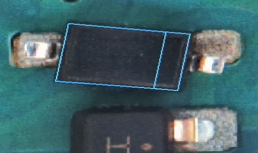
SuRFace Mount Technology (SMT) has become the backbone of modern electronic manufacturing, enabling the miniaturization and high-density assembly of electronic components. Among the most widely used SMT components are chip resistors and capacitors, with small form factors (01005, 0201, 0402) dominating compact product designs such as smartphones, wearables, and IoT devices. However, these miniature components are highly prone to a common assembly defect known as "billboarding" or "tombstoning"—a phenomenon where the component stands vertically on one end (like a tombstone) instead of lying flat on the PCB pads during reflow soldering. This defect disrupts electrical connections, causes functional failures, and increases rework costs, posing a significant challenge to mass production yields.
Billboarding in small resistors and capacitors is primarily driven by an imbalance in solder paste volume, wetting force, or thermal distribution between the two terminal pads of the component. While factors such as PCB pad design, component placement accuracy, and solder paste quality contribute to the defect, stencil aperture design and reflow soldering profile are two of the most controllable and impactful variables. This article provides a comprehensive analysis of SMT billboarding in small resistors and capacitors, focusing on how to mitigate the defect through targeted optimization of stencil aperture geometry and reflow curve parameters. It integrates industry standards (IPC-7525, IPC-A-610, IPC-J-STD-005) and practical case studies to validate the proposed optimization strategies, ensuring they are compliant and applicable to high-volume manufacturing environments.
1. Understanding SMT Component Billboarding: Mechanisms and Root Causes
Billboarding occurs when a chip resistor or capacitor rotates around one of its terminal pads during the reflow soldering process, resulting in the other pad being lifted off the PCB surface. This rotation is caused by an imbalance in the forces acting on the component’s two terminals, with the dominant force pulling one end downward while the other end is lifted. To effectively optimize stencil apertures and reflow profiles, it is critical to first understand the underlying mechanisms and root causes of the defect.
1.1 Core Mechanisms of Billboarding
The billboarding phenomenon is governed by three key physical mechanisms during reflow soldering: solder paste melting and wetting, surface tension forces, and thermal expansion mismatch. These mechanisms interact to create the force imbalance that drives component rotation:
- Solder Paste Wetting Imbalance: When solder paste melts, it wets the component terminal and PCB pad surfaces, forming a solder fillet. If one terminal wets faster or more completely than the other, the resulting surface tension force will pull that end of the component toward the pad, causing rotation around the slower-wetting terminal.
- Surface Tension Gradient: Unequal solder paste volume between the two pads creates a surface tension gradient. More solder paste on one pad generates a stronger surface tension force, pulling the component toward that pad and lifting the opposite end.
- Thermal Expansion Mismatch: Differential heating of the component or PCB pads causes uneven thermal expansion. For example, if one pad is closer to a large thermal mass (e.g., a BGA package), it will heat up slower, delaying solder paste melting and creating a wetting imbalance.
For small components (01005, 0201), these mechanisms are amplified due to their low mass (01005 components weigh ~0.002 grams) and small terminal area, making them highly sensitive to even minor force or thermal imbalances.
1.2 Root Causes of Billboarding in Small Resistors/Capacitors
While billboarding is a result of force or thermal imbalance, several root causes contribute to this imbalance. These causes can be categorized into four key areas: stencil aperture design, reflow profile parameters, PCB and component design, and process variables. Among these, stencil aperture design and reflow profile are the most amenable to optimization:
1.2.1 Stencil Aperture-Related Causes
Stencil aperture design directly controls the volume and distribution of solder paste deposited on the PCB pads. Poor aperture design is a leading cause of billboarding:
- Unequal Aperture Sizes: If the two apertures for a component’s terminals are of different sizes, they will deposit unequal solder paste volumes, creating a surface tension imbalance.
- Non-Optimal Aperture Aspect Ratio: For small components, an incorrect aspect ratio (aperture width/height) can lead to incomplete solder paste transfer or inconsistent volume deposition. The IPC-7525 standard recommends an aspect ratio of ≥1.5 for reliable solder paste transfer.
- Aperture Misalignment: Apertures that are not perfectly aligned with the PCB pads can cause solder paste to be deposited off-center, leading to uneven wetting and force imbalance.
- Stencil Thickness Inconsistency: Variations in stencil thickness (even ±0.01 mm) can result in significant solder paste volume differences between pads, especially for small apertures.
1.2.2 Reflow Profile-Related Causes
The reflow profile (temperature vs. time curve) governs the melting, wetting, and solidification of solder paste. An improperly designed profile can exacerbate wetting and thermal imbalances:
- Inadequate Preheat Stage: A short or low-temperature preheat stage fails to activate flux, leading to poor solder wetting. It also causes uneven heating of the PCB and components, creating thermal imbalances.
- Rapid Temperature Ramp-Up: A steep ramp-up rate (exceeding 3°C/sec) causes solder paste to melt unevenly, with one terminal’s paste melting faster than the other. This creates a wetting imbalance that drives rotation.
- Suboptimal Peak Temperature: A peak temperature that is too low (below the solder paste’s melting point + 10°C) results in incomplete wetting, while a temperature that is too high can degrade flux, leading to poor wetting and component damage.
- Insufficient Dwell Time: Inadequate time spent above the solder paste’s melting point (dwell time) prevents complete wetting and solder fillet formation, increasing the risk of billboarding.
1.2.3 Other Contributing Causes
While stencil and reflow optimization are the focus of this article, other factors can contribute to billboarding and should be addressed as part of a comprehensive defect mitigation strategy:
- PCB Pad Design: Unequal pad sizes, incorrect pad spacing, or contaminated pads (oxidation, flux residue) can cause wetting imbalances.
- Component Placement Accuracy: Components placed off-center or at an angle can lead to uneven solder paste contact and subsequent rotation.
- Solder Paste Quality: Solder paste with expired flux, incorrect viscosity, or uneven particle distribution can result in inconsistent wetting.
2. Stencil Aperture Design Optimization for Mitigating Billboarding
Stencil aperture design is the first line of defense against billboarding, as it directly controls solder paste volume and distribution. For small resistors and capacitors (01005, 0201, 0402), optimizing aperture geometry, size, and alignment is critical to ensuring balanced solder paste deposition and wetting. Below is a detailed breakdown of key optimization strategies, aligned with IPC-7525 (Stencil Design Guidelines) and industry best practices.
2.1 Core Principles of Aperture Design for Small Components
The primary goal of aperture design optimization is to deposit a consistent, balanced volume of solder paste on each of the component’s two terminals. This requires adherence to three core principles:
- Balanced Volume Deposition: The two apertures for a component’s terminals must be identical in size and shape to ensure equal solder paste volume.
- Optimal Aspect Ratio: The aperture aspect ratio (width/height) must be ≥1.5 to ensure reliable solder paste transfer. For small components with narrow pads, this may require adjusting stencil thickness.
- Precise Alignment: Apertures must be perfectly aligned with PCB pads to ensure solder paste is deposited centered on each pad, avoiding off-center wetting.
Stencil thickness is a foundational parameter that impacts aperture design. For small components, a stencil thickness of 0.10 mm (4 mils) is typically recommended, as it balances solder paste volume and transfer efficiency. Thicker stencils (0.12 mm) may be used for larger components (0402), but they increase the risk of excessive solder paste volume for 01005/0201 components.
2.2 Aperture Geometry Optimization
The geometry of the stencil aperture (shape, size, and spacing) has a significant impact on solder paste deposition and wetting. For small resistors and capacitors, the following geometry optimizations are recommended:
2.2.1 Aperture Shape: Rectangular vs. Round vs. Custom
Rectangular apertures are the most commonly used for chip resistors and capacitors, as they match the rectangular shape of the component’s terminals. However, slight modifications to the rectangular shape can improve solder paste transfer and wetting:
- Rectangular Apertures with Tapered Edges: Adding a slight taper (0.05-0.10 mm) to the aperture edges (on the stencil’s bottom surface, facing the PCB) improves solder paste release, reducing the risk of paste bridging or incomplete transfer. This is especially beneficial for 01005 components with narrow pads.
- Oval Apertures for Narrow Pads: For components with very narrow pads (e.g., 01005 resistors with 0.20 mm wide pads), oval apertures (slightly longer than the pad length) can increase solder paste volume without violating aspect ratio requirements. The oval shape ensures that the paste is evenly distributed across the pad, promoting balanced wetting.
- Avoid Round Apertures: Round apertures are not recommended for small rectangular components, as they deposit solder paste in a circular pattern that may not cover the entire terminal pad, leading to uneven wetting and billboarding.
2.2.2 Aperture Size Optimization
Aperture size directly determines the volume of solder paste deposited. For small components, the aperture size should be carefully matched to the PCB pad size to ensure balanced volume and avoid excessive or insufficient paste. The following guidelines are based on component form factor:
| Component Form Factor | PCB Pad Dimensions (Length × Width, mm) | Recommended Aperture Dimensions (Length × Width, mm) | Stencil Thickness (mm) | Estimated Solder Paste Volume per Pad (mm³) |
|---|---|---|---|---|
| 01005 (0.40×0.20 mm) | 0.35×0.18 | 0.32×0.16 (tapered edges) | 0.10 | 0.0051 |
| 0201 (0.60×0.30 mm) | 0.50×0.25 | 0.47×0.23 (tapered edges) | 0.10 | 0.0108 |
| 0402 (1.00×0.50 mm) | 0.90×0.45 | 0.85×0.42 (rectangular, no taper) | 0.10-0.12 | 0.0357-0.0428 |
Key considerations for aperture size optimization:
- Aperture Reduction Factor: The aperture size should be 5-10% smaller than the PCB pad size to prevent solder paste bridging between adjacent pads and ensure the paste is contained within the pad area. This reduction factor is critical for small components with tight pad spacing (e.g., 01005 components with 0.20 mm pad spacing).
- Balanced Apertures: The two apertures for a component’s terminals must be identical in size. Even a 0.01 mm difference in width can result in a 10%+ difference in solder paste volume, creating a surface tension imbalance.
- Aspect Ratio Check: For each aperture design, verify that the aspect ratio (width/thickness) is ≥1.5. For example, a 01005 aperture with a width of 0.16 mm and stencil thickness of 0.10 mm has an aspect ratio of 1.6, which meets the IPC-7525 requirement.
2.2.3 Aperture Spacing and Alignment
Aperture spacing (distance between the two apertures for a component’s terminals) and alignment with the PCB pads are critical to ensuring proper component placement and wetting:
- Aperture Spacing: The distance between the two apertures should match the distance between the component’s terminals (i.e., the component’s length minus twice the terminal width). For example, a 0201 component with a length of 0.60 mm and terminal width of 0.10 mm has a terminal spacing of 0.40 mm, so the aperture spacing should be 0.40 mm. Incorrect spacing can cause the component to be placed off-center, leading to uneven solder paste contact.
- Aperture Alignment: Apertures must be aligned with the PCB pads such that the solder paste is deposited centered on each pad. Misalignment (even ±0.02 mm) can cause the paste to be concentrated on one side of the pad, leading to uneven wetting and rotation. Stencil fabrication should use laser cutting with a precision of ±0.005 mm to ensure accurate alignment.
2.3 Advanced Aperture Design Techniques
For high-volume production or components with a history of billboarding, advanced aperture design techniques can further improve solder paste deposition and reduce defects:
2.3.1 Step Stencils
Step stencils (stencils with varying thicknesses in different regions) are useful when a PCB contains both small components (01005/0201) and larger components (0402/BGA) that require different solder paste volumes. The small component region uses a thinner stencil (0.10 mm) to avoid excessive paste, while the larger component region uses a thicker stencil (0.12-0.15 mm) to ensure sufficient paste. This prevents over-deposition on small components, which is a common cause of billboarding.
2.3.2 Laser-Cut vs. Electroformed Stencils
Laser-cut stencils are the most common for SMT assembly, but electroformed stencils offer superior precision for small apertures. Electroformed stencils have smoother aperture walls, which improve solder paste release and reduce the risk of paste residue buildup. For 01005 components, electroformed stencils (with aperture precision of ±0.003 mm) can significantly improve solder paste transfer consistency, reducing billboarding rates by 30-50% compared to laser-cut stencils.
2.3.3 Aperture Modifications for Thermal Imbalances
In cases where billboarding is caused by thermal imbalances (e.g., one pad is near a large thermal mass), slight aperture modifications can compensate for the uneven wetting. For example, increasing the size of the aperture on the slower-heating pad by 5-10% can deposit more solder paste, creating a stronger surface tension force that counteracts the thermal imbalance. This technique should be used cautiously, as over-modification can lead to bridging or excessive solder.
3. Reflow Soldering Profile Optimization for Mitigating Billboarding
The reflow soldering profile is the second critical variable for mitigating billboarding. A well-designed profile ensures uniform heating, complete flux activation, and balanced solder paste wetting—all of which are essential for preventing component rotation. Below is a detailed breakdown of reflow profile optimization, aligned with IPC-J-STD-005 (Solder Paste Specifications) and IPC-A-610 (Acceptability of Electronic Assemblies).
3.1 Overview of Reflow Profile Stages
A typical reflow soldering profile consists of four stages: preheat, soak (activation), reflow, and cooling. Each stage plays a critical role in solder paste behavior and component wetting. Optimization involves adjusting the temperature, time, and ramp rate of each stage to ensure balanced wetting and minimize thermal imbalances:
- Preheat Stage: Raises the PCB and components from room temperature to the flux activation temperature (typically 120-150°C) at a controlled ramp rate. This stage removes moisture and volatile components from the solder paste and activates the flux.
- Soak Stage: Maintains the temperature at the flux activation range to ensure complete flux activation and uniform heating of the PCB and components. This stage minimizes thermal gradients across the PCB.
- Reflow Stage: Raises the temperature above the solder paste’s melting point (T) to melt the solder and form a solder fillet. The peak temperature and dwell time (time above T) are critical for wetting and fillet formation.
- Cooling Stage: Cools the PCB and components at a controlled rate to solidify the solder fillet, ensuring good joint strength and avoiding thermal shock.
For small resistors and capacitors, the preheat, soak, and reflow stages are the most critical for mitigating billboarding, as they directly impact wetting and thermal balance.
3.2 Key Reflow Profile Parameters to Optimize
The following parameters should be optimized to prevent billboarding in small components. Recommendations are based on common lead-free solder pastes (Sn-Ag-Cu, T = 217°C):
3.2.1 Preheat Stage: Ramp-Up Rate and Temperature
The preheat stage’s ramp-up rate is a critical parameter for avoiding thermal imbalances. A steep ramp-up rate causes uneven heating, with components and pads closer to the reflow oven’s heating elements warming up faster than those in shadowed areas. For small components:
- Ramp-Up Rate: Maintain a ramp-up rate of 1-2°C/sec (maximum 2.5°C/sec) from room temperature to the soak temperature. This slow ramp ensures uniform heating of the PCB, components, and pads, minimizing thermal gradients.
- Preheat Temperature Range: Raise the temperature to 120-150°C (flux activation range) at the end of the preheat stage. This activates the flux, which cleans the component terminals and PCB pads, promoting good wetting.
- Preheat Duration: The preheat stage should last 60-120 seconds, depending on the PCB’s thermal mass. Thicker PCBs (≥1.6 mm) require a longer preheat time to ensure uniform heating.
A common mistake is using a rapid ramp-up rate to reduce cycle time, but this increases billboarding rates by 2-3x for 01005/0201 components.
3.2.2 Soak Stage: Temperature and Duration
The soak stage is designed to eliminate thermal imbalances and ensure complete flux activation. For small components, the soak stage parameters should be optimized as follows:
- Soak Temperature: Maintain a temperature of 150-170°C (slightly above the flux activation temperature) during the soak stage. This ensures that flux is fully activated and any remaining moisture is evaporated.
- Soak Duration: The soak stage should last 40-90 seconds. A longer soak time (up to 90 seconds) is recommended for PCBs with high thermal mass or dense component placement, as it helps equalize temperatures across the board.
- Temperature Uniformity: Ensure that the temperature variation across the PCB during the soak stage is ≤±5°C. This can be verified using a thermal profiler with multiple sensors placed near critical components (e.g., 01005 resistors, BGAs).
Insufficient soak time leads to incomplete flux activation and residual thermal imbalances, while excessive soak time can degrade the flux, leading to poor wetting.
3.2.3 Reflow Stage: Peak Temperature and Dwell Time
The reflow stage is where solder paste melts and wetting occurs. The peak temperature and dwell time are the most critical parameters for preventing billboarding:
- Peak Temperature: The peak temperature should be 240-250°C for Sn-Ag-Cu solder paste (23-33°C above T). This ensures complete melting of the solder paste and good wetting of the component terminals and PCB pads. A peak temperature below 235°C can result in incomplete wetting, while a temperature above 255°C can degrade the component’s package or PCB solder mask.
- Dwell Time: The dwell time (time above T = 217°C) should be 30-60 seconds. This provides sufficient time for the solder paste to melt, wet the pads and terminals, and form a uniform solder fillet. An insufficient dwell time (≤20 seconds) leads to incomplete wetting, while an excessive dwell time (≥70 seconds) can cause solder balling or component drift.
- Ramp-Up to Peak Temperature: Maintain a ramp-up rate of 1-2°C/sec from the soak temperature to the peak temperature. A steep ramp-up rate during this phase can cause uneven solder paste melting, creating a wetting imbalance.
3.2.4 Cooling Stage: Ramp-Down Rate
While the cooling stage does not directly cause billboarding, it impacts solder joint strength and component stability. A controlled ramp-down rate prevents thermal shock and ensures proper solder fillet formation:
- Ramp-Down Rate: Cool the PCB from the peak temperature to 150°C at a rate of 2-4°C/sec. This controlled cooling ensures that the solder solidifies uniformly, reducing the risk of solder joint cracks.
- Final Cooling: Allow the PCB to cool to room temperature naturally or using forced air (at ≤25°C) after the reflow stage. Avoid quenching the PCB in cold water, as this can cause thermal shock and component damage.
3.3 Profile Optimization for Specific Component Form Factors
Smaller components require more precise profile optimization due to their higher sensitivity to thermal and wetting imbalances. Below are tailored recommendations for common small component form factors:
3.3.1 01005 Components (0.40×0.20 mm)
01005 components are the most prone to billboarding due to their ultra-small size and low mass. The following profile parameters are recommended:
- Preheat: Ramp-up rate 1-1.5°C/sec, temperature 120-140°C, duration 90-120 seconds.
- Soak: Temperature 150-160°C, duration 60-90 seconds, temperature uniformity ≤±3°C.
- Reflow: Ramp-up rate 1°C/sec, peak temperature 240-245°C, dwell time 30-45 seconds.
- Cooling: Ramp-down rate 2-3°C/sec.
The slower ramp-up and lower peak temperature help prevent uneven melting and component drift.
3.3.2 0201 Components (0.60×0.30 mm)
0201 components are slightly more robust than 01005 but still require careful profile optimization:
- Preheat: Ramp-up rate 1.5-2°C/sec, temperature 130-150°C, duration 60-90 seconds.
- Soak: Temperature 150-170°C, duration 40-70 seconds, temperature uniformity ≤±4°C.
- Reflow: Ramp-up rate 1.5°C/sec, peak temperature 245-250°C, dwell time 40-50 seconds.
- Cooling: Ramp-down rate 2-4°C/sec.
3.3.3 0402 Components (1.00×0.50 mm)
0402 components are larger and less prone to billboarding, but profile optimization still improves yields:
- Preheat: Ramp-up rate 2-2.5°C/sec, temperature 140-160°C, duration 40-60 seconds.
- Soak: Temperature 160-170°C, duration 30-50 seconds, temperature uniformity ≤±5°C.
- Reflow: Ramp-up rate 2°C/sec, peak temperature 245-250°C, dwell time 45-60 seconds.
- Cooling: Ramp-down rate 3-4°C/sec.
4. Validation and Testing of Optimization Strategies
After optimizing stencil apertures and reflow profiles, it is critical to validate the improvements through standardized testing. This ensures that the optimization strategies effectively reduce billboarding rates and do not introduce new defects (e.g., bridging, cold solder joints). Below are key validation methods:
4.1 Defect Rate Monitoring
Monitor billboarding rates before and after optimization using statistical process control (SPC) tools. For high-volume production, inspect at least 500 PCBs per lot and track the number of billboarded components. A successful optimization should reduce billboarding rates by ≥70% for 01005/0201 components and ≥50% for 0402 components.
4.2 Thermal Profiling
Use a thermal profiler (e.g., KIC Explorer, Datapaq) to verify the reflow profile parameters. Place multiple sensors (5-10) across the PCB, including near critical small components and thermal masses. Ensure that the measured profile matches the optimized parameters (ramp rates, temperatures, durations) and that temperature uniformity is within the required range.
4.3 Solder Paste Volume Measurement
Measure the solder paste volume deposited by the optimized stencil using a solder paste inspection (SPI) machine. Verify that the volume is consistent between the two pads of each component (variation ≤5%) and matches the target volume (see Table 1). SPI data can also identify aperture misalignment or paste transfer issues.
4.4 Visual and X-Ray Inspection
Conduct visual inspection of solder joints using a stereo microscope (10-50x magnification) to check for billboarding, bridging, cold solder joints, and solder fillet quality. For hidden joints (e.g., components under BGAs), use X-ray inspection to verify solder joint integrity. Ensure that solder fillets are uniform, with ≥75% pad coverage (per IPC-A-610).
4.5 Reliability Testing
Perform reliability tests to ensure that optimized stencil and reflow parameters do not compromise solder joint reliability. Common tests include: Thermal Cycle Testing: Subject PCBs to -40°C to 125°C thermal cycles (1000 cycles) to test solder joint fatigue resistance.Vibration Testing: Apply random vibration (10-2000 Hz, 3 g acceleration) to simulate transportation conditions and test joint robustness.Solder Joint Shear Testing: Measure the shear strength of solder joints using a universal testing machine. The shear strength should meet IPC-J-STD-006 requirements (≥1.5 N for 01005 components).
5. Case Study: Billboarding Mitigation in 0201 Components
A consumer electronics manufacturer was experiencing a 8% billboarding rate in 0201 chip capacitors (100 nF, 0603 package equivalent) on a smartphone PCB assembly line. The root cause analysis identified two key issues: unequal stencil aperture sizes and a rapid reflow ramp-up rate. The following optimization strategies were implemented:
5.1 Stencil Aperture Optimization
- Changed stencil aperture size from 0.45×0.22 mm (unbalanced, left aperture 0.45×0.22 mm, right aperture 0.43×0.22 mm) to 0.47×0.23 mm (balanced, identical apertures for both terminals).
- Added tapered edges (0.05 mm) to the apertures to improve solder paste release.
- Reduced stencil thickness from 0.12 mm to 0.10 mm to avoid excessive solder paste volume.
5.2 Reflow Profile Optimization
- Reduced the preheat ramp-up rate from 3°C/sec to 1.5°C/sec.
- Increased the soak duration from 30 seconds to 60 seconds to improve temperature uniformity.
- Adjusted the peak temperature from 255°C to 245°C and dwell time from 25 seconds to 45 seconds.
5.3 Optimization Results
After implementing the optimizations, the manufacturer achieved the following results:Billboarding rate reduced from 8% to 0.5% (93.75% reduction).Solder paste volume variation between pads reduced from 12% to 3%.Temperature uniformity during soak stage improved from ±8°C to ±3°C.Annual rework costs reduced by $150,000.Production yield increased from 91% to 99.2%.
This case study demonstrates that targeted optimization of stencil apertures and reflow profiles can effectively mitigate billboarding in small SMT components, significantly improving production yields and reducing costs.
6. Common Optimization Mistakes and How to Avoid Them
Even with careful planning, common mistakes can undermine stencil and reflow optimization efforts. Below are the most frequent mistakes and mitigation strategies:
6.1 Over-Optimizing Aperture Size
Mistake: Increasing aperture size to compensate for billboarding, leading to excessive solder paste volume and bridging between adjacent pads. Solution: Maintain aperture size at 5-10% smaller than the PCB pad size. Use tapered edges or oval apertures to improve paste transfer without increasing size. Verify solder paste volume with SPI before scaling up production.
6.2 Ignoring Thermal Uniformity
Mistake: Focusing only on peak temperature and dwell time, while neglecting temperature uniformity during preheat and soak stages. Solution: Use a thermal profiler with multiple sensors to map temperature distribution across the PCB. Adjust preheat and soak parameters to ensure uniformity ≤±5°C. For high-thermal-mass PCBs, use a longer soak time.
6.3 Using a One-Size-Fits-All Profile
Mistake: Applying the same reflow profile to all PCBs, regardless of component density or thermal mass. Solution: Develop tailored profiles for different PCB designs. For example, a PCB with dense 01005 components requires a slower ramp-up rate than a PCB with larger components. Store profiles in the reflow oven’s memory for easy selection.
6.4 Neglecting Stencil Maintenance
Mistake: Failing to clean or inspect the stencil regularly, leading to paste buildup, clogged apertures, or worn edges. Solution: Implement a stencil maintenance schedule: clean the stencil after every 500-1000 prints, inspect apertures for wear or clogging daily, and replace the stencil after 50,000-100,000 prints (or earlier if wear is detected).
7. Conclusion
Billboarding in small SMT resistors and capacitors (01005, 0201, 0402) is a costly defect that can be effectively mitigated through targeted optimization of stencil aperture design and reflow soldering profiles. By understanding the root causes of billboarding—primarily solder paste volume imbalance and thermal/wetting imbalances—manufacturers can implement focused optimizations to ensure balanced paste deposition and uniform heating.
Stencil aperture optimization involves balancing aperture size, geometry, and alignment to ensure equal solder paste volume on each component terminal. Key strategies include using tapered rectangular or oval apertures, maintaining a 5-10% aperture reduction factor relative to PCB pads, and ensuring an aspect ratio ≥1.5. Advanced techniques such as step stencils or electroformed stencils can further improve paste transfer consistency for high-volume production.
Reflow profile optimization focuses on controlling ramp rates, temperatures, and durations to minimize thermal imbalances and ensure complete wetting. Critical parameters include a slow preheat ramp-up rate (1-2°C/sec), sufficient soak time (40-90 seconds) for temperature uniformity, and a well-controlled reflow stage (peak temperature 240-250°C, dwell time 30-60 seconds).
Validation through defect rate monitoring, thermal profiling, SPI, and reliability testing is essential to confirm the effectiveness of optimization strategies. By implementing these approaches, manufacturers can significantly reduce billboarding rates, improve production yields, and lower rework costs—critical for success in the competitive electronics manufacturing landscape.