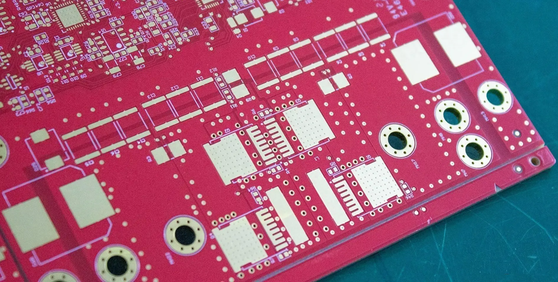
 PCB
PCB FPC
FPC Rigid-Flex
 FR-4
FR-4 HDI PCB
 Rogers High-Frequency Board
 PTFE Teflon High-Frequency Board
 Aluminum
 Copper Core
 PCB Assembly
 LED light PCBA
 Memory PCBA
 Power Supply PCBA
 New Energey PCBA
 Communication PCBA
 Industrial Control PCBA
 Medical Equipment PCBA
 Testing Service
 PCBA Testing Service
 Certification Application
 RoHS Certification Application
 REACH Certification Application
 CE Certification Application
 FCC Certification Application
 CQC Certification Application
 UL Certification Application
 Transformers, Inductors
 High Frequency Transformers
 Low Frequency Transformers
 High Power Transformers
 Conversion Transformers
 Sealed Transformers
 Ring Transformers
 Inductors
 Wires,Cables Customized
 Network Cables
 Power Cords
 Antenna Cables
 Coaxial Cables
 Net Position Indicator
 Solar AIS net position indicator
 Capacitors
 Connectors
 Diodes
 Embedded Processors & Controllers
 Digital Signal Processors (DSP/DSC)
 Microcontrollers (MCU/MPU/SOC)
 Programmable Logic Device(CPLD/FPGA)
 Communication Modules/IoT
 Resistors
 Through Hole Resistors
 Resistor Networks, Arrays
 Potentiometers,Variable Resistors
 Aluminum Case,Porcelain Tube Resistance
 Current Sense Resistors,Shunt Resistors
 Switches
 Transistors
 Power Modules
 Isolated Power Modules
 AC-DC Power Modules
 DC-AC Module(Inverter)
 RF and Wireless
Minimum Distance Between RF Connector Pad Edges and PCB Board Edges to Avoid Signal Reflection
2025-12-03
RF connectors are critical interfaces in high-frequency electronic systems (e.g., 5G, Wi-Fi 6E, radar, satellite communications), enabling reliable signal transmission between PCBs and external devices. A frequently overlooked but impactful design detail is the distance between RF connector pad edges and Pcb Board edges—referred to as the "edge clearance." Insufficient edge clearance disrupts the impedance continuity of the RF signal path, triggering signal reflection, which degrades key performance metrics like return loss (RL), insertion loss (IL), and bit error rate (BER). This article comprehensively analyzes the relationship between edge clearance, impedance discontinuity, and signal reflection, defines minimum distance requirements aligned with IPC-2222 and RF design best practices, and provides actionable design guidelines to ensure impedance matching and signal integrity in RF systems operating at 1–60 GHz.
1. Fundamentals of RF Signal Reflection and Impedance Continuity
To understand why edge clearance matters, it is essential to establish the core principles of RF signal propagation and reflection:
1.1 RF Signal Propagation and Impedance
RF signals travel along PCB transmission lines (e.g., microstrip, stripline) as transverse electromagnetic (TEM) waves, where the characteristic impedance (Z₀) of the line determines signal behavior. For most RF systems, the target Z₀ is 50Ω (industry standard for impedance matching between connectors, cables, and active components). Z₀ is governed by:
- Transmission line geometry (trace width, dielectric thickness),
- Dielectric constant (Dk) of the PCB substrate,
- Ground plane configuration,
- Proximity to PCB edges or other metallic structures.
Any deviation from the target Z₀ creates an impedance discontinuity, causing a portion of the RF signal to reflect back toward the source (signal reflection), while the remainder transmits forward.
1.2 Signal Reflection Metrics and Impact
Reflection is quantified by return loss (RL), measured in decibels (dB): RL (dB) = 20 × log₁₀ (|Γ|) Where Γ (reflection coefficient) = (Z_discontinuity - Z₀) / (Z_discontinuity + Z₀).
- Acceptable RL: For most RF applications (e.g., 5G base stations, Wi-Fi routers), RL ≤ -15 dB is required (meaning <3% of the signal is reflected). Critical applications (e.g., radar, satellite) demand RL ≤ -20 dB (<1% reflection).
- Impact of poor RL: Reflected signals interfere with the incident signal, causing:
- Signal distortion (e.g., amplitude ripple in frequency response),
- Reduced power delivery to the load,
- Increased electromagnetic interference (EMI) due to signal leakage,
- System instability (e.g., oscillator drift in transceivers).
PCB board edges introduce impedance discontinuity by altering the electromagnetic field distribution around the RF connector pad—making edge clearance a key factor in minimizing reflection.
2. How PCB Board Edges Cause Impedance Discontinuity
The RF connector pad (and its associated transmission line) relies on a stable electromagnetic field between the pad/trace and the underlying ground plane. When the pad edge is too close to the PCB board edge, two primary effects disrupt this field, leading to Z₀ deviation:
2.1 Fringing Field Distortion
RF signals generate fringing fields that extend laterally from the pad/trace beyond its physical width. These fields are normally confined by the surrounding dielectric and ground plane. However:
- Near-board-edge placement: If the pad edge is <3× the dielectric thickness from the board edge, the fringing fields "escape" into the air (instead of interacting with the dielectric/ground plane). Air has a lower Dk (≈1) than typical PCB substrates (FR-4 Dk = 4.2–4.5; Rogers 4350 Dk = 3.48), reducing the effective Dk seen by the signal.
- Z₀ increase: A lower effective Dk increases Z₀ (Z₀ ∝ √(1/Dk)). For example, a 50Ω microstrip trace on FR-4 (dielectric thickness = 0.8mm) with a pad edge 0.5mm from the board edge may see Z₀ jump to 58Ω—a discontinuity that causes Γ = (58-50)/(58+50) ≈ 0.07, RL ≈ -23 dB (marginal for critical apps) if uncompensated. Closer edges (0.2mm) push Z₀ to 65Ω, Γ ≈ 0.13, RL ≈ -17 dB (unacceptable for 5G).
2.2 Ground Plane Current Crowding
RF currents flow in the ground plane directly beneath the pad/trace (displacement current). When the pad is near the board edge:
- Ground plane truncation: The board edge cuts off the ground plane beneath the pad’s outer edge, forcing ground currents to crowd into a smaller area.
- Increased ground impedance: Current crowding raises the ground plane’s impedance, creating a voltage drop that adds to the signal’s effective impedance (Z_total = Z_trace + Z_ground). This further increases Z_discontinuity and reflection.
For surface-mount RF connectors (e.g., SMA, SMB, U.FL), the pad’s ground pins exacerbate this effect—truncated ground near the board edge reduces the contact area between the connector’s ground lug and the PCB, increasing ground bounce and reflection.
3. Minimum Edge Clearance Requirements: Standards and Simulation Data
The minimum distance between RF connector pad edges and PCB board edges depends on three factors: RF frequency, PCB dielectric thickness, and connector type. Below are requirements derived from IPC-2222 (Section 6.3, "Board Edge Clearances for High-Frequency Components") and 3D electromagnetic (EM) simulation (using ANSYS HFSS) for common RF scenarios:
3.1 Frequency-Dependent Clearance
Higher frequencies increase the wavelength (λ) of the RF signal, making the system more sensitive to small impedance discontinuities. The edge clearance should scale with λ/20 (a rule of thumb to ensure the discontinuity is "electrically small" and minimally reflective):
| RF Frequency (GHz) | Wavelength (λ) in Air (mm) | λ/20 (mm) | Minimum Edge Clearance (mm) |
|---|---|---|---|
| 1–6 | 300–50 | 15–2.5 | 3.0 |
| 6–18 | 50–16.7 | 2.5–0.83 | 4.0 |
| 18–40 | 16.7–7.5 | 0.83–0.375 | 5.0 |
| 40–60 | 7.5–5.0 | 0.375–0.25 | 6.0 |
Note: For frequencies >60 GHz (mmWave), clearance should be ≥8.0mm due to extreme sensitivity to field distortion.
3.2 Dielectric Thickness Impact
Thicker dielectrics (h) increase the vertical extent of fringing fields, requiring larger edge clearance to prevent field escape. The minimum clearance should be ≥3h to contain fringing fields:
| PCB Dielectric Thickness (h, mm) | 3h (mm) | Minimum Edge Clearance (mm) |
|---|---|---|
| 0.4 (thin FR-4) | 1.2 | 3.0 (frequency <6GHz) |
| 0.8 (standard FR-4) | 2.4 | 4.0 (frequency 6–18GHz) |
| 1.6 (thick FR-4/Rogers) | 4.8 | 5.0 (frequency 18–40GHz) |
| 2.4 (high-power RF PCBs) | 7.2 | 8.0 (frequency >40GHz) |
3.3 Connector Type Considerations
Different RF connector types (surface-mount vs. through-hole, large vs. miniaturized) have varying pad sizes and field distributions, affecting clearance needs:
- Surface-mount (SMT) connectors (e.g., SMA, U.FL): Their pads are smaller and closer to the board surface, making fringing fields more vulnerable to edge effects. Minimum clearance = 4.0–6.0mm (depending on frequency).
- Through-hole (PTH) connectors (e.g., N-type, TNC): Their pads extend through the PCB, with ground planes on both sides, reducing field escape. Minimum clearance = 3.0–5.0mm.
- Miniaturized connectors (e.g., MMCX, SMP): Their tiny pads (0.5–1.0mm width) have concentrated fringing fields—require 5.0–7.0mm clearance to avoid reflection.
3.4 Validation via EM Simulation
A 3D HFSS simulation of a 24GHz Wi-Fi 6E system (FR-4, h=0.8mm, Z₀=50Ω) with an SMA connector pad shows:
- Clearance = 2.0mm: Z₀ = 62Ω, Γ = 0.11, RL = -18.3 dB (fails -20dB requirement).
- Clearance = 4.0mm: Z₀ = 53Ω, Γ = 0.03, RL = -29.5 dB (meets critical app requirements).
- Clearance = 6.0mm: Z₀ = 51Ω, Γ = 0.01, RL = -40 dB (negligible reflection).
This confirms that increasing clearance beyond the minimum further improves RL, with diminishing returns above 6.0mm for most frequencies.
4. Design Guidelines to Optimize Edge Clearance and Reduce Reflection
Meeting the minimum edge clearance is necessary but not sufficient—integrate these design practices to ensure impedance continuity and minimal reflection:
4.1 Pad and Transmission Line Co-Design
- Pad-trace impedance matching: The RF connector pad should have the same Z₀ as the connected transmission line. For a 50Ω microstrip trace (width = 1.2mm on FR-4, h=0.8mm), the pad should be 1.2mm wide (same as the trace) to avoid a step discontinuity. Taper the pad to the trace width over a length of ≥2× the trace width (2.4mm) if the pad is larger than the trace.
- Ground plane extension: Extend the ground plane beneath the connector pad to within 0.1mm of the pad edge. Avoid ground plane cuts or slots near the pad—these create additional impedance discontinuities.
4.2 Edge Profiling and PCB Material Selection
- Smooth board edges: Use CNC routing to create smooth, burr-free board edges near the RF pad. Rough edges (Ra >1.0μm) scatter fringing fields, increasing reflection.
- High-Dk substrates: For applications where edge clearance is limited (e.g., compact IoT devices), use substrates with higher Dk (e.g., Rogers 4535, Dk=3.66) to reduce fringing field extent. A higher Dk concentrates fields closer to the pad, minimizing escape at smaller clearances.
- Thinner dielectrics: If space allows, use thinner dielectrics (h=0.4mm) to reduce 3h clearance requirements. For example, h=0.4mm reduces 3h to 1.2mm, allowing a minimum clearance of 3.0mm for 6GHz signals.
4.3 Shielding and Grounding
- Edge shielding: For PCBs with limited edge clearance (<minimum requirement), add a metallic shield (e.g., copper tape, aluminum frame) along the board edge adjacent to the RF pad. The shield acts as a "virtual ground plane," containing fringing fields and restoring Z₀. Ensure the shield is connected to the PCB’s main ground plane via low-impedance vias (0.3mm diameter, spaced 1mm apart).
- Ground vias around the pad: Place a ring of ground vias (0.4mm diameter) around the RF connector pad, 0.5mm from the pad edge. These vias short the top and bottom ground planes, reducing ground impedance and suppressing field escape. Space vias every 1.5–2mm for frequencies <20GHz, and every 1mm for >20GHz.
4.4 Connector Placement Best Practices
- Avoid corner placement: Do not place RF connectors at PCB corners—corner edges create two perpendicular field escape paths, doubling the impedance discontinuity. Place connectors along straight board edges instead.
- Distance from other components: Keep non-RF components (e.g., resistors, capacitors) at least 3mm away from the RF pad edge. Metallic components (e.g., inductors, ICs) reflect fringing fields, adding to impedance distortion.
- Symmetric placement: For differential RF signals (e.g., MIPI D-PHY), place the two connector pads symmetrically relative to the board edge (same clearance for both) to maintain differential impedance balance.
5. Validation and Testing of Edge Clearance and Reflection
To confirm that edge clearance meets requirements and reflection is minimized, implement these validation steps:
5.1 Impedance Measurement
- TDR (Time-Domain Reflectometry): Use a TDR oscilloscope to measure the impedance profile of the RF path. A flat impedance line (±2Ω of Z₀) indicates no significant discontinuity. A peak in impedance at the pad-edge location confirms insufficient clearance.
- VNA (Vector Network Analyzer): Measure RL over the operating frequency range. Ensure RL ≤ -15 dB (or -20 dB for critical apps) across all frequencies. A dip in RL (poorer performance) at specific frequencies indicates resonance from edge-induced discontinuities.
5.2 EM Simulation
- 3D Field Simulation: Use HFSS or CST Studio Suite to simulate the RF pad and board edge. Visualize fringing fields to confirm they are contained within the dielectric (no escape to air). Adjust clearance until Z₀ is within ±1Ω of the target.
- Parameter Sweeps: Sweep edge clearance from 1mm to 8mm in simulations to identify the minimum clearance that achieves acceptable RL. This helps optimize space while meeting performance goals.
5.3 Prototype Testing
- Bench Testing: Assemble prototypes with varying edge clearances (e.g., 2mm, 4mm, 6mm) and measure RL using a VNA. Compare results to simulations to validate the design.
- Environmental Testing: Test prototypes under temperature (-40°C to 85°C) and humidity (85% RH) conditions. Thermal expansion of the PCB can slightly alter edge clearance—ensure RL remains stable over the operating range.
6. Conclusion
The minimum distance between RF connector pad edges and PCB board edges is a critical design parameter for avoiding signal reflection in high-frequency systems. Requirements scale with RF frequency, dielectric thickness, and connector type—ranging from 3.0mm for 1–6GHz signals on thin dielectrics to 8.0mm for >60GHz mmWave signals on thick substrates. Insufficient clearance disrupts fringing fields and ground current distribution, causing impedance discontinuities that degrade RL and signal integrity.
By following IPC-2222 guidelines, leveraging EM simulation, and integrating design practices like pad-trace matching, edge shielding, and ground vias, engineers can ensure impedance continuity and minimize reflection. Validation via TDR, VNA, and prototype testing confirms that edge clearance meets performance goals, even in compact RF devices where space is limited. This attention to detail is essential for the reliable operation of modern RF systems, where signal integrity directly impacts range, data rate, and overall system performance.