 PCB
PCB FPC
FPC Rigid-Flex
 FR-4
FR-4 HDI PCB
 Rogers High-Frequency Board
 PTFE Teflon High-Frequency Board
 Aluminum
 Copper Core
 PCB Assembly
 LED light PCBA
 Memory PCBA
 Power Supply PCBA
 New Energey PCBA
 Communication PCBA
 Industrial Control PCBA
 Medical Equipment PCBA
 Testing Service
 PCBA Testing Service
 Certification Application
 RoHS Certification Application
 REACH Certification Application
 CE Certification Application
 FCC Certification Application
 CQC Certification Application
 UL Certification Application
 Transformers, Inductors
 High Frequency Transformers
 Low Frequency Transformers
 High Power Transformers
 Conversion Transformers
 Sealed Transformers
 Ring Transformers
 Inductors
 Wires,Cables Customized
 Network Cables
 Power Cords
 Antenna Cables
 Coaxial Cables
 Net Position Indicator
 Solar AIS net position indicator
 Capacitors
 Connectors
 Diodes
 Embedded Processors & Controllers
 Digital Signal Processors (DSP/DSC)
 Microcontrollers (MCU/MPU/SOC)
 Programmable Logic Device(CPLD/FPGA)
 Communication Modules/IoT
 Resistors
 Through Hole Resistors
 Resistor Networks, Arrays
 Potentiometers,Variable Resistors
 Aluminum Case,Porcelain Tube Resistance
 Current Sense Resistors,Shunt Resistors
 Switches
 Transistors
 Power Modules
 Isolated Power Modules
 AC-DC Power Modules
 DC-AC Module(Inverter)
 RF and Wireless
Layout Strategies for Standard Resistors (0402, 0603) to Minimize Interference with Adjacent Signals
2025-12-19
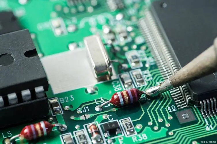
Standard chip resistors with 0402 (1.0mm × 0.5mm) and 0603 (1.6mm × 0.8mm) packages are ubiquitous in modern electronic designs, valued for their small size, low cost, and compatibility with high-volume suRFace-mount assembly. They serve critical functions such as current limiting, voltage division, and signal termination in applications ranging from consumer electronics (smartphones, laptops) to industrial control systems and telecommunications equipment. However, despite their passive nature, these resistors can act as sources or propagators of electromagnetic interference (EMI) if not properly laid out on the printed circuit board (PCB). Interference from poorly placed resistors can degrade signal integrity (SI), increase bit error rates, and even cause system malfunctions—especially in high-speed designs (≥100 MHz) where signal wavelengths become comparable to PCB feature sizes. This article provides a comprehensive analysis of how standard resistors contribute to signal interference, and outlines evidence-based layout strategies aligned with industry standards (IPC-2221, IPC-6012) to mitigate these effects. It focuses on 0402 and 0603 packages, exploring parasitic characteristics, interference mechanisms, and practical layout techniques for reducing crosstalk, radiated EMI, and ground bounce.
1. Fundamental Understanding: Why Resistors Cause Signal Interference
To effectively mitigate interference through layout, it is first essential to recognize that real-world resistors are not ideal. Beyond their nominal resistance value, they exhibit parasitic capacitance and inductance, which become significant at high frequencies. These parasitic components, combined with the resistor’s physical placement relative to signal traces, ground planes, and other components, give rise to interference.
1.1 Parasitic Characteristics of Standard Resistors
All chip resistors—including 0402 and 0603 packages—have inherent parasitic parameters that deviate from ideal behavior: Parasitic Inductance (L): Arises from the resistor’s lead frames, termination electrodes, and the current path through the resistive material. For 0402 resistors, L typically ranges from 0.5 to 1.5 nH; for 0603 resistors, it is slightly higher (1.0 to 2.0 nH). At frequencies above 100 MHz, this inductance becomes significant, transforming the resistor into an R-L network. This inductance can resonate with parasitic capacitance, creating impedance peaks that reflect high-frequency signals.Parasitic Capacitance (C): Exists between the resistor’s two termination electrodes (inter-terminal capacitance) and between each electrode and the PCB’s ground plane (pad capacitance). Inter-terminal capacitance for 0402 and 0603 resistors is typically 0.1 to 0.3 pF. At high frequencies, this capacitance provides a low-impedance path for signal coupling between the resistor’s terminals and adjacent traces.Thermal Noise: All resistors generate thermal (Johnson-Nyquist) noise, which is proportional to their resistance value, temperature, and bandwidth. While thermal noise is inherent and cannot be eliminated by layout, poor placement can couple this noise into sensitive signal paths (e.g., analog circuits).
1.2 Key Interference Mechanisms Involving Resistors
Resistors contribute to signal interference through three primary mechanisms, all of which are strongly influenced by layout: Crosstalk: The transfer of signal energy from one trace to another through capacitive or inductive coupling. Resistors act as "coupling bridges" when placed between adjacent signal traces—their parasitic capacitance and inductance enhance the electromagnetic coupling between the traces. For example, a 0603 resistor placed parallel to two closely spaced high-speed signal traces can increase crosstalk by 10–15 dB at 500 MHz.Radiated EMI: High-frequency currents flowing through the resistor (and its associated traces) generate electromagnetic fields that radiate into the surrounding environment. These fields can interfere with sensitive components (e.g., radio receivers, analog-to-digital converters). The radiation intensity increases with the length of the current path (including the resistor’s terminals and connecting traces) and the frequency of the current.Ground Bounce: When a resistor is connected to a ground plane with a long or narrow trace, switching currents through the resistor can cause voltage fluctuations (ground bounce) on the plane. This bounce propagates to other components connected to the same ground plane, degrading their performance. Resistors used in current-limiting applications (e.g., for LED drivers or logic gates) are particularly prone to causing ground bounce if their ground connections are not optimized.
The severity of these interference mechanisms depends on the resistor’s package size (0603 resistors, with larger dimensions, typically exhibit higher parasitic inductance/capacitance than 0402), the signal frequency, and the proximity of the resistor to sensitive traces or components. Layout design directly addresses these factors by minimizing coupling paths, reducing current loop areas, and optimizing ground connections.
2. Core Layout Principles for Reducing Resistor-Induced Interference
The foundation of interference mitigation for 0402 and 0603 resistors lies in three core layout principles: minimizing current loop areas, maximizing spacing between resistors and sensitive signals, and optimizing ground connections. These principles apply to all resistor applications and form the basis for more specific layout strategies discussed in subsequent sections.
2.1 Minimize Current Loop Areas
The inductance of a current loop is proportional to the area of the loop—larger loops generate stronger magnetic fields and are more susceptible to inductive coupling. For resistors, the current loop includes the resistor itself, the traces connecting it to other components, and the return path through the ground plane. To minimize loop area: Use Short, Wide Traces: Connect the resistor to other components with the shortest possible traces (preferably ≤2mm for high-frequency signals). Wide traces (≥0.4mm for 0402 resistors, ≥0.6mm for 0603) reduce resistance and inductance, minimizing the loop’s impedance. Avoid meandering or "staircase" traces, which increase loop length and area.Align Resistors with Current Flow: Place the resistor such that its length axis is parallel to the direction of current flow. This reduces the effective length of the current path through the resistor, minimizing parasitic inductance. For example, if current flows from left to right along a trace, place the 0402 resistor (which has a longer length dimension) horizontally, so the current travels along the resistor’s length rather than its width.Minimize Via Usage: Vias introduce inductance (≈0.5–1 nH per via) and increase loop area if used unnecessarily. If the resistor must be placed on a different layer than the signal trace, use a single via for each connection (power and ground) and place the vias as close to the resistor’s pads as possible.
2.2 Maximize Spacing Between Resistors and Sensitive Signals
Capacitive and inductive coupling between a resistor and adjacent signal traces decreases with the square of the distance between them. Increasing spacing is one of the most effective ways to reduce crosstalk. Guidelines for spacing:Follow IPC-2221 Spacing Requirements: IPC-2221 specifies minimum spacing between components and traces based on voltage and signal type. For high-frequency signals (≥100 MHz), exceed the minimum spacing by 50–100%. For example, if the minimum spacing for a 3.3V signal is 0.2mm, use 0.3–0.4mm spacing between the resistor and the signal trace.Separate Digital and Analog Resistors: Digital resistors (e.g., those used in logic circuits) carry high-frequency switching currents that generate significant EMI. Analog resistors (e.g., those in sensor circuits or op-amp feedback loops) are sensitive to noise. Place digital and analog resistors on separate sides of the PCB or separated by a ground plane to prevent cross-contamination.Avoid Placing Resistors Over Signal Traces: In multi-layer PCBs, do not place resistors on the top layer directly above high-speed signal traces on inner layers. The resistor’s parasitic capacitance can couple noise between the top layer and the inner trace, even through the PCB substrate.
2.3 Optimize Ground Connections
Poor ground connections for resistors can create ground bounce and increase loop inductance. To optimize ground connections: Connect Resistor Ground Pads Directly to Ground Planes: For resistors that connect to ground (e.g., termination resistors, pull-down resistors), connect their ground pad to the nearest ground plane using a short via. Avoid connecting the ground pad to a ground trace that meanders across the PCB, as this increases the return path length.Use Star Grounding for Resistor Networks: If multiple resistors (e.g., a voltage divider) share a common ground connection, connect them to a single ground point (star configuration) rather than dAISy-chaining their ground traces. This prevents current from one resistor from causing voltage drops in the ground path of another resistor.Ensure Ground Plane Continuity: Avoid splitting the ground plane near resistors, as this forces return currents to flow around the split, increasing loop area and inductance. If a ground plane split is necessary (e.g., for analog/digital isolation), use a single point of connection (ground bridge) near the resistor to minimize return path length.
3. Application-Specific Layout Strategies for 0402 and 0603 Resistors
Resistors are used in a variety of applications, each with unique interference risks. The following sections outline layout strategies tailored to common resistor applications, with a focus on 0402 and 0603 packages.
3.1 Termination Resistors for High-Speed Signals
Termination resistors (e.g., 50Ω or 100Ω) are used to match the impedance of high-speed signal traces (e.g., USB 3.0, HDMI, Ethernet) to prevent signal reflection. Poorly placed termination resistors can cause significant crosstalk and reflection. Layout strategies: Place Termination Resistors as Close to the Load as Possible: The optimal placement for a termination resistor is within 1–2mm of the load component’s signal pin. This minimizes the length of the unterminated trace segment, reducing reflection and crosstalk. For 0402 resistors (smaller size), this is easier to achieve than for 0603 resistors, making 0402 preferable for high-density, high-speed designs.Align Resistors with Differential Pairs: For differential signal pairs (e.g., USB 3.0), place termination resistors (if used) symmetrically relative to the pair. Ensure that the traces from the resistor to each differential pin are of equal length to maintain impedance balance. Avoid placing the resistor between the two differential traces, as this can disrupt the pair’s symmetry.Minimize Trace Length Between Resistor and Ground: For parallel termination (resistor between signal and ground), the trace from the resistor to the ground via should be as short as possible (≤1mm). This reduces the loop area of the termination circuit, minimizing radiated EMI.Example: In a USB 3.2 Gen 2 design (10 Gbps), a 0402 50Ω termination resistor should be placed within 1mm of the USB controller’s signal pin. The resistor’s ground pad should be connected to the ground plane via a via located directly under the pad, with no trace between the pad and the via.
3.2 Voltage Divider Resistors
Voltage dividers are used to generate reference voltages or scale input signals. They are common in analog circuits and power management systems, where noise coupling can degrade accuracy. Layout strategies: Place Resistors Close Together: The two resistors in a voltage divider should be placed as close to each other as possible (≤2mm apart) to minimize the length of the trace between them. This reduces the area of the current loop formed by the divider, minimizing inductive coupling from external signals.Locate the Divider Near the Load: Place the voltage divider as close to the component that uses the divided voltage as possible. This reduces the length of the trace carrying the low-voltage reference signal, which is highly sensitive to noise.Shield the Divider from High-Frequency Traces: If the voltage divider is used in an analog circuit, place it in a shielded area of the PCB (surrounded by a ground plane) to isolate it from high-frequency digital traces. Avoid placing the divider within 5mm of digital clock traces or switching power supply components.Example: A voltage divider using two 0603 10kΩ resistors to generate a 1.65V reference for an ADC should be placed within 3mm of the ADC’s reference pin. The divider should be surrounded by a ground plane, with no digital traces within 5mm of the resistors.
3.3 Current-Limiting Resistors
Current-limiting resistors (e.g., for LEDs, MOSFET gates, or logic inputs) control the flow of current to prevent component damage. They can generate ground bounce and radiated EMI if not properly laid out. Layout strategies: Place Resistors Close to the Load Component: For LED current-limiting resistors, place the resistor as close to the LED’s anode or cathode as possible. For MOSFET gate resistors, place the resistor within 1mm of the gate pin. This minimizes the length of the high-current trace, reducing radiated EMI.Optimize Ground Return Paths: The ground return path for the current-limiting resistor should be as short as possible. Connect the resistor’s ground pad directly to the load component’s ground pin (e.g., LED cathode to ground) rather than to a distant ground node. This reduces ground bounce by minimizing the voltage drop along the return path.Avoid Placing Resistors in High-Speed Signal Paths: Current-limiting resistors for digital components (e.g., logic gate inputs) should not be placed in the middle of high-speed signal traces. If possible, place the resistor at the driver end of the trace to minimize the length of the trace carrying the limited current.Example: A 0402 220Ω current-limiting resistor for an LED should be placed within 1mm of the LED’s anode. The resistor’s ground connection (via the LED’s cathode) should be a short trace (≤2mm) to the nearest ground via.
3.4 Pull-Up/Pull-Down Resistors
Pull-up (connected to VCC) and pull-down (connected to ground) resistors set the default state of digital signals. They can contribute to crosstalk if placed too close to adjacent signal traces. Layout strategies: Place Resistors Close to the Signal Pin: Pull-up/pull-down resistors should be placed within 2mm of the component’s signal pin. This minimizes the length of the trace between the resistor and the pin, reducing the area available for crosstalk coupling.Route Power/Ground Traces Away from Sensitive Signals: For pull-up resistors, the trace connecting the resistor to VCC should be routed away from sensitive signal traces (e.g., analog inputs). Similarly, the ground trace for pull-down resistors should be kept separate from analog ground traces.Avoid Parallel Placement with Adjacent Signals: Do not place pull-up/pull-down resistors parallel to adjacent high-speed signal traces. If possible, place the resistor perpendicular to the trace to minimize the overlapping area between the resistor and the trace, reducing capacitive coupling.Example: A 0603 10kΩ pull-up resistor for an I2C SDA pin should be placed within 2mm of the I2C controller’s SDA pin. The trace from the resistor to VCC should be routed away from the I2C SCL trace, with a minimum spacing of 0.4mm between the two traces.
4. Additional Layout Techniques for Interference Mitigation
Beyond application-specific strategies, several additional layout techniques can further reduce resistor-induced interference, particularly for 0402 and 0603 packages in high-density, high-frequency designs.
4.1 Using Ground Planes Effectively
Ground planes are the most effective tool for reducing EMI and crosstalk in PCB designs. For resistors: Use a Solid Ground Plane Under Resistors: In multi-layer PCBs, place a solid ground plane directly below the resistor layer. This provides a low-impedance return path for current, minimizes loop inductance, and shields the resistor from interference from inner-layer traces.Avoid Cutting Ground Planes Under Resistors: Do not route traces through the ground plane under resistors, as this creates "holes" that increase inductance and reduce shielding effectiveness. If a trace must cross under a resistor, use a narrow trace and ensure it is perpendicular to the resistor’s current path.Implement Guard Rings for Sensitive Resistors: For resistors in analog circuits (e.g., op-amp feedback resistors), surround the resistor with a guard ring connected to ground. The guard ring acts as a shield, preventing noise from coupling into the resistor’s traces.
4.2 Optimizing Trace Routing Around Resistors
The way traces are routed around resistors can significantly impact interference: Avoid Right-Angle Traces Near Resistors: Right-angle traces have higher inductance and radiate more EMI than 45° or curved traces. When routing traces to/from resistors, use 45° angles or smooth curves to minimize inductance.Keep Traces Symmetric for Differential Pairs: When routing differential traces past resistors, ensure that the distance from each trace to the resistor is equal. This maintains the pair’s impedance balance and reduces common-mode noise.Minimize Trace Length Between Resistors and Vias: If a resistor’s trace must transition to another layer via a via, place the via as close to the resistor’s pad as possible (≤1mm). This reduces the length of the trace segment that is not supported by the ground plane, minimizing inductance.
4.3 Selecting the Right Resistor Package (0402 vs. 0603)
The choice between 0402 and 0603 packages can impact interference: 0402 Resistors for High-Frequency, High-Density Designs: 0402 resistors have smaller parasitic inductance and capacitance than 0603 resistors, making them better suited for high-frequency signals (≥500 MHz). Their small size also allows for closer placement to component pins, minimizing trace length and loop area.0603 Resistors for Higher Power or Easier Assembly: 0603 resistors can handle higher power dissipation (typically 0.1W vs. 0.063W for 0402) and are easier to assemble in low-volume production (better solderability). They are suitable for lower-frequency applications (≤100 MHz) where parasitic effects are less significant.Guideline: For signals above 100 MHz, use 0402 resistors whenever possible. For power applications or low-frequency signals, 0603 resistors are acceptable and may be preferred for manufacturing ease.
5. Validation and Testing of Resistor Layouts
After implementing the layout strategies outlined above, validation is essential to ensure that interference is minimized. For 0402 and 0603 resistors, validation can be performed using simulation tools and physical testing.
5.1 Simulation Tools
PCB design software with SI/EMI simulation capabilities (e.g., Altium Designer, Cadence Allegro, Mentor PADS) can predict the impact of resistor layout on signal integrity: Crosstalk Simulation: Simulate crosstalk between a resistor and adjacent signal traces to verify that the spacing and layout are sufficient. The simulation should show crosstalk levels below -30 dB for high-speed signals (≥100 MHz).Impedance Simulation: For termination resistors, simulate the impedance of the trace-resistor network to ensure it matches the target impedance (e.g., 50Ω). Parasitic inductance and capacitance of the resistor and traces should be included in the simulation.Radiated EMI Simulation: Use 3D EM simulation tools (e.g., Ansys HFSS) to predict radiated EMI from resistor circuits. The simulation should confirm that EMI levels comply with regulatory standards (e.g., FCC Part 15, CISPR 22).
5.2 Physical Testing
For prototype PCBs, physical testing validates simulation results: Signal Integrity Testing: Use an oscilloscope with a high-bandwidth probe (≥1 GHz) to measure signal waveforms at the load component. Check for reflection, overshoot, and crosstalk. For high-speed signals, the signal should maintain a clean waveform with overshoot/undershoot below 10% of the nominal voltage.EMI Testing: Conduct radiated EMI testing in an anechoic chamber to measure the EMI emitted by the PCB. The measured EMI levels should be below the limits specified by the relevant standard (e.g., FCC Part 15 Class B for consumer electronics).Ground Bounce Testing: Use an oscilloscope to measure voltage fluctuations on the ground plane near the resistor. Ground bounce should be below 5% of the nominal supply voltage.
6. Common Layout Mistakes to Avoid
Even with careful planning, common layout mistakes can negate the benefits of proper resistor placement. The following are key mistakes to avoid: Placing Resistors Too Far from Component Pins: A termination resistor placed 5mm from the load pin can increase reflection by 20–30% at 500 MHz, degrading signal integrity.Using Narrow Traces for Resistor Connections: Narrow traces (≤0.2mm) increase inductance and resistance, creating larger current loops and more radiated EMI.Mixing Analog and Digital Resistors in the Same Area: Placing an analog voltage divider resistor near a digital clock trace can couple clock noise into the analog signal, reducing the ADC’s accuracy.Ignoring Parasitic Parameters in Simulation: Simulating resistors as ideal components (no parasitic inductance/capacitance) can lead to over-optimistic SI predictions. Always include parasitic parameters in simulations.Overcrowding Resistors in High-Density Areas: Placing multiple resistors too close together (≤0.2mm apart) increases mutual inductance and capacitance between them, leading to cross-coupling.
7. Conclusion
Standard 0402 and 0603 resistors, while passive, can significantly impact signal integrity and generate EMI if not properly laid out on the PCB. The key to minimizing interference lies in understanding the resistor’s parasitic characteristics and implementing layout strategies that minimize current loop areas, maximize spacing from sensitive signals, and optimize ground connections. Application-specific strategies—tailored to termination, voltage divider, current-limiting, and pull-up/pull-down resistors—further enhance interference mitigation. By selecting the appropriate resistor package (0402 for high-frequency, 0603 for power/ease of assembly) and validating the layout through simulation and testing, engineers can ensure that resistors do not degrade system performance.