 PCB
PCB FPC
FPC Rigid-Flex
 FR-4
FR-4 HDI PCB
 Rogers High-Frequency Board
 PTFE Teflon High-Frequency Board
 Aluminum
 Copper Core
 PCB Assembly
 LED light PCBA
 Memory PCBA
 Power Supply PCBA
 New Energey PCBA
 Communication PCBA
 Industrial Control PCBA
 Medical Equipment PCBA
 Testing Service
 PCBA Testing Service
 Certification Application
 RoHS Certification Application
 REACH Certification Application
 CE Certification Application
 FCC Certification Application
 CQC Certification Application
 UL Certification Application
 Transformers, Inductors
 High Frequency Transformers
 Low Frequency Transformers
 High Power Transformers
 Conversion Transformers
 Sealed Transformers
 Ring Transformers
 Inductors
 Wires,Cables Customized
 Network Cables
 Power Cords
 Antenna Cables
 Coaxial Cables
 Net Position Indicator
 Solar AIS net position indicator
 Capacitors
 Connectors
 Diodes
 Embedded Processors & Controllers
 Digital Signal Processors (DSP/DSC)
 Microcontrollers (MCU/MPU/SOC)
 Programmable Logic Device(CPLD/FPGA)
 Communication Modules/IoT
 Resistors
 Through Hole Resistors
 Resistor Networks, Arrays
 Potentiometers,Variable Resistors
 Aluminum Case,Porcelain Tube Resistance
 Current Sense Resistors,Shunt Resistors
 Switches
 Transistors
 Power Modules
 Isolated Power Modules
 AC-DC Power Modules
 DC-AC Module(Inverter)
 RF and Wireless
Evaluating Crystallographic Quality of Blind Via Bottom Copper Layers via Metallographic Cross-Section Analysis
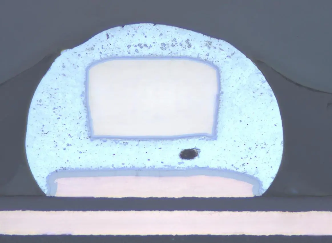
In Hdi Pcb manufacturing, the crystallographIC quality of blind via bottom copper layers critically impacts interconnection reliability. Coarse grains or abnormal textures accelerate electromigration and reduce mechanical strength. Metallographic cross-section analysis combined with microscopy enables quantitative evaluation of grain size, orientation, and defects.
1. Sample Preparation
1.1 Sectioning and Mounting
-
Precision cutting: Diamond wire saw aligned perpendicular to via axis (≤5μm error, Figure 1);
-
Cold mounting: Low-shrinkage epoxy (e.g., EpoFix™) under vacuum, cured at 25℃×24h.
1.2 Grinding and Polishing
-
Coarse grinding: SiC paper (#320→#1200) with water cooling;
-
Fine polishing:
-
Initial: 3μm diamond suspension, 150rpm×5min;
-
Final: 0.05μm silica colloid, 100rpm×2min (Ra<0.01μm).
-
2. Microstructure Visualization
2.1 Chemical Etching
-
Etchant: Fe(NO₃)₃ (10g) + ethanol (100ml) + H₂O (50ml);
-
Conditions: 15-30s immersion at 25℃ (gray-level contrast >30%, Figure 2).
2.2 EBSD Analysis
-
Sample preparation: Ion polishing (5kV×2h) to remove damage;
-
Scanning: 0.1μm step size, 20kV, IPF-Z mapping.
3. Crystallographic Metrics
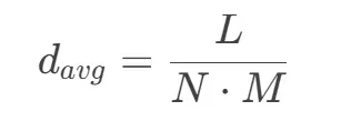
3.1 Grain Size Measurement
-
Line-intercept method: Draw 5 random lines (total 500μm), calculate average grain size:
where L=total length, N=intersections, M=magnification.
3.2 Texture Coefficient
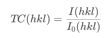
-
ODF analysis: Calculate pole densities for (111)/(200) planes:
TC>3 indicates strong anisotropy.
3.3 Defect Quantification
-
Porosity: ImageJ analysis of dark area ratio (<0.5% required);
-
Twin density: Annealing twins counted per mm² (normal range:50-200/mm²).
4. Case Study
Server motherboard blind via analysis:
-
Grain size: 8.2μm (plated at 2ASD, additive A=5ml/L);
-
Texture: TC(111)=2.1, TC(200)=1.3 (weak texture);
-
Porosity: 0.12%;
-
Reliability: <2% resistance change after 1000 thermal cycles (-55℃~125℃).
Conclusion
Metallographic cross-section analysis with quantitative imaging provides precise evaluation of copper layer crystallography, guiding plating process optimization to ensure long-term reliability in high-density interconnects.