 PCB
PCB FPC
FPC Rigid-Flex
 FR-4
FR-4 HDI PCB
 Rogers High-Frequency Board
 PTFE Teflon High-Frequency Board
 Aluminum
 Copper Core
 PCB Assembly
 LED light PCBA
 Memory PCBA
 Power Supply PCBA
 New Energey PCBA
 Communication PCBA
 Industrial Control PCBA
 Medical Equipment PCBA
 Testing Service
 PCBA Testing Service
 Certification Application
 RoHS Certification Application
 REACH Certification Application
 CE Certification Application
 FCC Certification Application
 CQC Certification Application
 UL Certification Application
 Transformers, Inductors
 High Frequency Transformers
 Low Frequency Transformers
 High Power Transformers
 Conversion Transformers
 Sealed Transformers
 Ring Transformers
 Inductors
 Wires,Cables Customized
 Network Cables
 Power Cords
 Antenna Cables
 Coaxial Cables
 Net Position Indicator
 Solar AIS net position indicator
 Capacitors
 Connectors
 Diodes
 Embedded Processors & Controllers
 Digital Signal Processors (DSP/DSC)
 Microcontrollers (MCU/MPU/SOC)
 Programmable Logic Device(CPLD/FPGA)
 Communication Modules/IoT
 Resistors
 Through Hole Resistors
 Resistor Networks, Arrays
 Potentiometers,Variable Resistors
 Aluminum Case,Porcelain Tube Resistance
 Current Sense Resistors,Shunt Resistors
 Switches
 Transistors
 Power Modules
 Isolated Power Modules
 AC-DC Power Modules
 DC-AC Module(Inverter)
 RF and Wireless
The Importance and Manufacturing Process of Medical PCBs
The Importance and Manufacturing Process of Medical PCBs
Medical Pcbs (Printed Circuit Boards) serve as crucial components in medical equipment and facilities, underscoring their immense importance. In the medical field, the precision of every device and facility is directly linked to the safety and well-being of patients. As medical equipment is used on people, the stakes are incredibly high, necessitating the utmost accuracy and reliability in their underlying PCBs.
Applications of Medical PCBs
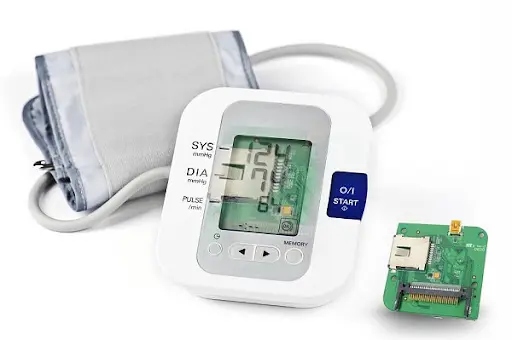
Medical PCBs find their way into a wide array of medical devices, including heart monitors, blood glucose monitors, blood pressure monitors, X-ray CT scanners, and pacemakers. These devices rely on the precision and stability of their PCBs to ensure accurate and life-saving functionalities.
Advantages of Medical PCBs
Medical PCBs offer numerous advantages that enhance healthcare delivery and patient outcomes:
Mobile Health: With smartphones, tablets, and smartwatches equipped with health-monitoring capabilities, medical professionals can seamlessly send and receive vital information. These devices also facilitate medication orders and research, streamlining healthcare processes.
Health Record Management: Medical PCBs enable electronic record-keeping, eliminating the need for manual data entry. This accelerates treatment processes and reduces errors, ultimately saving lives.
Wireless Communication: Medical systems powered by PCBs facilitate the transmission and reception of critical medical information, allowing patients to access lab results from home. Mobile devices and web-based applications further enhance this convenience by helping users locate nearby hospitals, pharmacies, and other medical facilities.
Data-Driven Medication: Medical PCBs facilitate the rapid and efficient production of medications tailored to specific patient populations. Advanced medical devices assist in data collection, accelerating drug development processes.
Wearable Devices: Medical PCBs underpin wearable devices that monitor users' health conditions, providing vital information to medical professionals for effective treatments. Athletes and sportspeople also use such devices to track their performance and vital signs.
Designing and Manufacturing Medical PCBs
Medical PCBs must undergo meticulous design and manufacturing processes to ensure their high quality, reliability, robustness, and durability. The key steps involved in this process are:
Create Initial Schematic Design: Gather all relevant PCB information from clients and use it to create a basic schematic design. Details such as PCB application, type, power requirements, and materials are crucial for this stage.
Prepare Layout: Upload the preliminary schematic design to PCB software and incorporate client-specific details.
Consider and Add Critical Factors: Incorporate essential design elements like plane segmentation, sequencing, and pin selection to produce precise and effective PCBs.
Proper Power Segmentation: Divide power planes to minimize noise and crosstalk levels on the board.
Allow Multilayer Design: Implement a multilayer structure to reduce signal-to-noise ratio (SNR) and noise levels, enhancing PCB reliability and performance.
Review BOM (Bill of Materials): Compile a list of all materials and components required for the PCB.
Inspect Components: Thoroughly check PCB components to ensure they meet design specifications.
Prepare and Verify Spare Component List: Prepare a list of spare components to address potential failures or design mismatches, saving time during the design process.
Create Assembly Drawings: Develop detailed drawings for the PCB assembly process to ensure precision and accuracy.
Indicate Test Points in the Design: To ensure the accuracy of medical PCBs, indicate all potential test points during the design phase for effective testing.

Medical PCB Prototyping
Before mass production, a prototype of the medical PCB is created to assess its performance and identify potential issues. The prototyping process involves:
Creating the PCB design
Drafting the schematic design
Developing the routing design
Generating film for printing
Printing inner layers of the board
Laminating layers
Drilling holes
Imaging outer layers
Copper plating
Tin plating
Etching
Applying solder mask
Providing surface treatment
Adding silkscreen layers
Through these comprehensive steps, medical PCBs are designed and manufactured to meet the stringent standards of the medical field, ensuring reliability, accuracy, and cost-effectiveness in large-scale production.